- 您现在的位置:买卖IC网 > PDF目录375259 > ADM8696AN (ANALOG DEVICES INC) bqTINY-II Dual Input USB/AC Adpater 1-Cell Li-Ion Charger w/Term Enable & Temp Sense in QFN-10 10-SON -40 to 125 PDF资料下载
参数资料
| 型号: | ADM8696AN |
| 厂商: | ANALOG DEVICES INC |
| 元件分类: | 电源管理 |
| 英文描述: | bqTINY-II Dual Input USB/AC Adpater 1-Cell Li-Ion Charger w/Term Enable & Temp Sense in QFN-10 10-SON -40 to 125 |
| 中文描述: | 1-CHANNEL POWER SUPPLY MANAGEMENT CKT, PDIP16 |
| 封装: | PLASTIC, MS-001AB, DIP-16 |
| 文件页数: | 9/12页 |
| 文件大小: | 195K |
| 代理商: | ADM8696AN |
ADM8696/ADM8697
REV. 0
–9–
APPLICAT IONS INFORMAT ION
Increasing the Drive Current (ADM8696)
If the continuous output current requirements at V
OUT
exceeds
100 mA or if a lower V
CC
–V
OUT
voltage differential is desired,
an external PNP pass transistor may be connected in parallel
with the internal transistor. T he BAT T ON output (ADM8696)
can directly drive the base of the external transistor.
BATTERY
+5V
INPUT
POWER
0.1
μ
F
PNP
TRANSISTOR
0.1
μ
F
V
OUT
V
CC
BATT
ON
V
BATT
ADM8696
Figure 14. Increasing the Drive Current
Using a Rechargeable Battery for Backup (ADM8696)
If a capacitor or a rechargeable battery is used for backup, the
charging resistor should be connected to V
OUT
since this elimi-
nates the discharge path that would exist during power-down if
the resistor is connected to V
CC
.
V
OUT
V
CC
RECHARGABLE
BATTERY
+5V
INPUT
POWER
0.1
μ
F
0.1
μ
F
V
BATT
ADM8696
R
R
V
OUT
– V
BATT
I =
Figure 15. Rechargeable Battery
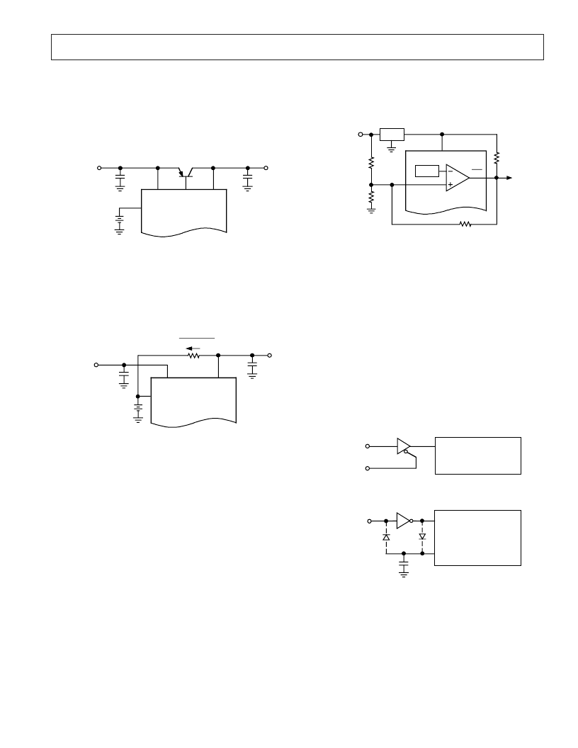
Adding Hysteresis to the Power Fail Comparator
For increased noise immunity, hysteresis may be added to the
power fail comparator. Since the comparator circuit is nonin-
verting, hysteresis can be added by connecting a resistor be-
tween the PFO output and the PFI input as shown in Fig-
ure 16. When PFO is low, resistor R3 sinks current from the
summing junction at the PFI pin. When PFO is high, the series
combination of R3 and R4 source current into the PFI summing
junction. T his results in differing trip levels for the comparator.
Alternate Watchdog Input Drive Circuits
T he watchdog feature can be enabled and disabled under pro-
gram control by driving WDI with a three-state buffer (Figure
17a). When three-stated, the WDI input will float, thereby dis-
abling the watchdog timer.
T his circuit is not entirely foolproof and it is possible a software
fault could erroneously three-state the buffer. T his would pre-
vent the ADM869x from detecting that the microprocessor is no
longer operating correctly. In most cases, a better method is to
ADM869x
R2
1.3V
R1
PFO
7805
R4
R3
+7V TO +15V
INPUT
POWER
+5V
PFI
V
CC
TO
μ
P NMI
V
H
= 1.3V
(
1+ R
)
V
L
= 1.3V
(
1+ R
)
2
ASSUMING R
4 < <
R
3
THEN
HYSTERESIS V
H
– V
L
= 5V
(
R
)
1
R
2
R
1
R
3
R
1
1
R
2
R
1
(5V – 1.3V)
1.3V (R
3 +
R
4
)
Figure 16. Adding Hysteresis to the Power Fail Comparator
extend the watchdog period rather than disabling the watchdog.
T his may be done under program control using the circuit
shown in Figure 17b. When the control input is high, the OSC
SEL pin is low and the watchdog timeout is set by the external
capacitor. A 0.01
μ
F capacitor sets a watchdog timeout delay of
100 s. When the control input is low, the OSC SEL pin is
driven high, selecting the internal oscillator. T he 100 ms or the
1.6 s period is chosen, depending on which diode in Fig-
ure 17b is used. With D1 inserted, the internal timeout is set at
100 ms while with D2 inserted the timeout is set at 1.6 s.
WDI
ADM869x
WATCHDOG
STROBE
CONTROL
INPUT
Figure 17a. Programming the Watchdog Input
OSC IN
OSC SEL
ADM869x
CONTROL
INPUT*
D1
D2
*LOW = INTERNAL TIMEOUT
HIGH = EXTERNAL TIMEOUT
Figure 17b. Programming the Watchdog Input
相关PDF资料 |
PDF描述 |
|---|---|
| ADM8696ARU | bqTINY-II Dual Input USB/AC Adpater 1-Cell Li-Ion Charger w/Term Enable & Temp Sense in QFN-10 10-SON -40 to 125 |
| ADM8696ARW | bqTINY-II Dual Input USB/AC Adpater 1-Cell Li-Ion Charger w/Charge Enable & Temp Sense, 7hr Timer 10-SON -40 to 85 |
| ADM8697AN | bqTINY-II Dual Input USB/AC Adpater 1-Cell Li-Ion Charger w/Timer Enable & Temp Sense, No Taper 10-SON -40 to 85 |
| ADM8697ARU | bqTINY-II Dual Input USB/AC Adpater 1-Cell Li-Ion Charger w/Timer Enable & Temp Sense, No Taper 10-SON -40 to 85 |
| ADM8697ARW | bqTINY-II Dual Input USB/AC Adpater 1-Cell Li-Ion Charger w/Charge Enable & AC Present, No Taper 10-SON -40 to 85 |
相关代理商/技术参数 |
参数描述 |
|---|---|
| ADM8696ANZ | 功能描述:IC SUPERVSR MPU ADJ/RESET 16DIP RoHS:是 类别:集成电路 (IC) >> PMIC - 监控器 系列:- 标准包装:1 系列:- 类型:简单复位/加电复位 监视电压数目:1 输出:开路漏极或开路集电极 复位:高有效 复位超时:- 电压 - 阀值:1.8V 工作温度:-40°C ~ 125°C 安装类型:表面贴装 封装/外壳:6-TSOP(0.059",1.50mm 宽)5 引线 供应商设备封装:5-TSOP 包装:剪切带 (CT) 其它名称:NCP301HSN18T1GOSCT |
| ADM8696ARU | 制造商:AD 制造商全称:Analog Devices 功能描述:Microprocessor Supervisory Circuits |
| ADM8696ARU-REEL | 功能描述:Supervisor Push-Pull, Push-Pull 1 Channel 16-TSSOP 制造商:analog devices inc. 系列:- 包装:带卷(TR) 零件状态:上次购买时间 类型:备用电池电路 受监控电压数:1 输出:推挽式,推挽式 复位:高有效/低有效 复位超时:最小为 35 ms 电压 - 阈值:1.3V 工作温度:-40°C ~ 85°C(TA) 安装类型:表面贴装 封装/外壳:16-TSSOP(0.173",4.40mm 宽) 供应商器件封装:16-TSSOP 标准包装:1 |
| ADM8696ARW | 功能描述:IC SUPERVSR MPU ADJ/RESET 16SOIC RoHS:否 类别:集成电路 (IC) >> PMIC - 监控器 系列:- 标准包装:1 系列:- 类型:简单复位/加电复位 监视电压数目:1 输出:开路漏极或开路集电极 复位:高有效 复位超时:- 电压 - 阀值:1.8V 工作温度:-40°C ~ 125°C 安装类型:表面贴装 封装/外壳:6-TSOP(0.059",1.50mm 宽)5 引线 供应商设备封装:5-TSOP 包装:剪切带 (CT) 其它名称:NCP301HSN18T1GOSCT |
| ADM8696ARW-REEL | 功能描述:IC SUPERVSR MPU ADJ/RESET 16SOIC RoHS:否 类别:集成电路 (IC) >> PMIC - 监控器 系列:- 标准包装:1 系列:- 类型:简单复位/加电复位 监视电压数目:1 输出:开路漏极或开路集电极 复位:高有效 复位超时:- 电压 - 阀值:1.8V 工作温度:-40°C ~ 125°C 安装类型:表面贴装 封装/外壳:6-TSOP(0.059",1.50mm 宽)5 引线 供应商设备封装:5-TSOP 包装:剪切带 (CT) 其它名称:NCP301HSN18T1GOSCT |
发布紧急采购,3分钟左右您将得到回复。