- 您现在的位置:买卖IC网 > PDF目录375259 > ADM8696ARU (ANALOG DEVICES INC) bqTINY-II Dual Input USB/AC Adpater 1-Cell Li-Ion Charger w/Term Enable & Temp Sense in QFN-10 10-SON -40 to 125 PDF资料下载
参数资料
| 型号: | ADM8696ARU |
| 厂商: | ANALOG DEVICES INC |
| 元件分类: | 电源管理 |
| 英文描述: | bqTINY-II Dual Input USB/AC Adpater 1-Cell Li-Ion Charger w/Term Enable & Temp Sense in QFN-10 10-SON -40 to 125 |
| 中文描述: | 1-CHANNEL POWER SUPPLY MANAGEMENT CKT, PDSO16 |
| 封装: | MO-153AB, TSSOP-16 |
| 文件页数: | 10/12页 |
| 文件大小: | 195K |
| 代理商: | ADM8696ARU |
ADM8696/ADM8697
REV. 0
–10–
T Y PICAL APPLICAT IONS
ADM8696
Figure 18 shows the ADM8696 in a typical power monitoring,
battery backup application. V
OUT
powers the CMOS RAM.
Under normal operating conditions with V
CC
present, V
OUT
is
internally connected to V
CC
. If a power failure occurs, V
CC
will
decay and V
OUT
will be switched to V
BAT T
, thereby maintaining
power for the CMOS RAM.
Power Fail
RESET
T he V
CC
power supply is also monitored by the Low Line In-
put, LL
IN
. A
RESET
pulse is generated when LL
IN
falls below
1.3 V.
RESET
will remain low for 50 ms after LL
IN
returns
above 1.3 V. T his allows for a power-on reset and prevents re-
peated toggling of
RESET
if the V
CC
power supply is unstable.
Resistors R3 and R4 should be chosen to give the desired V
CC
reset threshold.
Watchdog T imer
T he Watchdog T imer Input (WDI) monitors an I/O line from
the
μ
P system. T his line must be toggled once every 1.6 s to
verify correct software execution. Failure to toggle the line indi-
cates that the
μ
P system is not correctly executing its program
and may be tied up in an endless loop. If this happens, a reset
pulse is generated to initialize the processor.
If the watchdog timer is not needed the WDI input should be
left floating.
Power Fail Detector
T he Power Fail Input, PFI, monitors the input power supply via
a resistive divider network R1 and R2. T his input is intended as
an early warning power fail input. T he voltage on the PFI input
is compared with a precision 1.3 V internal reference. If the in-
put voltage drops below 1.3 V, a power fail output (PFO) signal
is generated. T his warns of an impending power failure and may
be used to interrupt the processor so that the system may be
shut down in an orderly fashion. T he resistors in the sensing
network are ratioed to give the desired power fail threshold volt-
age V
T
. T he threshold should be set at a higher voltage than the
RESET threshold so there is sufficient time available to com-
plete the shutdown procedure before the processor is RESET
and power is lost.
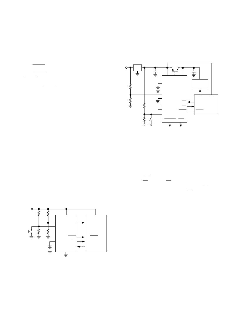
ADM8696
R2
R1
PFO
+5V
V
CC
CMOS RAM
POWER
I/O LINE
μ
P NMI
μ
P SYSTEM
μ
P POWER
V
OUT
WDI
GND
PFI
V
BATT
BATTERY
RESET
μ
P RESET
+
R4
R3
LL
IN
RESET
Figure 18a. ADM8696 Typical Application Circuit A
Figure 18b shows a similar application for the ADM8696 but in
this case the PFI input monitors the unregulated input to the
7805 voltage regulator. T his gives an earlier warning of an im-
pending power failure. It is useful with processors operating at
low speeds or where there are a significant number of house-
keeping tasks to be completed before the power is lost.
ADM8696
R2
R1
PFO
INPUT
POWER
V
CC
V
OUT
GND
PFI
V
BATT
0.1
μ
F
3V
BATTERY
RESET
OSC IN
OSC SEL
SYSTEM STATUS
INDICATORS
LOW LINE
CMOS RAM
I/O LINE
NMI
RESET
A0–A15
μ
P
BATT
ON
NC
V
CC
LL
IN
WDI
μ
P
POWER
RESET
R4
R3
7805
WDO
0.1
μ
F
Figure 18b. ADM8696 Typical Application Circuit B
T his application also shows an optional external transistor that
may be used to provide in excess of 100 mA current on V
OUT
.
When V
CC
is higher than V
BAT T
, the BAT T ON output goes
low, providing 25 mA of base drive for the external PNP transis-
tor. T he maximum current available is dependent on the power
rating of the external transistor.
RAM Write Protection
T he ADM8697
CE
OUT
line drives the Chip Select inputs of the
CMOS RAM.
CE
OUT
follows
CE
IN
as long as LL
IN
is above the
reset threshold. If LL
IN
falls below the reset threshold,
CE
OUT
goes high, independent of the logic level at
CE
IN
. T his prevents
the microprocessor from writing erroneous data into RAM dur-
ing power-up, power-down, brownouts and momentary power
interruptions.
相关PDF资料 |
PDF描述 |
|---|---|
| ADM8696ARW | bqTINY-II Dual Input USB/AC Adpater 1-Cell Li-Ion Charger w/Charge Enable & Temp Sense, 7hr Timer 10-SON -40 to 85 |
| ADM8697AN | bqTINY-II Dual Input USB/AC Adpater 1-Cell Li-Ion Charger w/Timer Enable & Temp Sense, No Taper 10-SON -40 to 85 |
| ADM8697ARU | bqTINY-II Dual Input USB/AC Adpater 1-Cell Li-Ion Charger w/Timer Enable & Temp Sense, No Taper 10-SON -40 to 85 |
| ADM8697ARW | bqTINY-II Dual Input USB/AC Adpater 1-Cell Li-Ion Charger w/Charge Enable & AC Present, No Taper 10-SON -40 to 85 |
| ADM8698AN | bqTINY-II Dual Input USB/AC Adpater 1-Cell Li-Ion Charger w/Charge Enable & AC Present, No Taper 10-SON -40 to 85 |
相关代理商/技术参数 |
参数描述 |
|---|---|
| ADM8696ARU-REEL | 功能描述:Supervisor Push-Pull, Push-Pull 1 Channel 16-TSSOP 制造商:analog devices inc. 系列:- 包装:带卷(TR) 零件状态:上次购买时间 类型:备用电池电路 受监控电压数:1 输出:推挽式,推挽式 复位:高有效/低有效 复位超时:最小为 35 ms 电压 - 阈值:1.3V 工作温度:-40°C ~ 85°C(TA) 安装类型:表面贴装 封装/外壳:16-TSSOP(0.173",4.40mm 宽) 供应商器件封装:16-TSSOP 标准包装:1 |
| ADM8696ARW | 功能描述:IC SUPERVSR MPU ADJ/RESET 16SOIC RoHS:否 类别:集成电路 (IC) >> PMIC - 监控器 系列:- 标准包装:1 系列:- 类型:简单复位/加电复位 监视电压数目:1 输出:开路漏极或开路集电极 复位:高有效 复位超时:- 电压 - 阀值:1.8V 工作温度:-40°C ~ 125°C 安装类型:表面贴装 封装/外壳:6-TSOP(0.059",1.50mm 宽)5 引线 供应商设备封装:5-TSOP 包装:剪切带 (CT) 其它名称:NCP301HSN18T1GOSCT |
| ADM8696ARW-REEL | 功能描述:IC SUPERVSR MPU ADJ/RESET 16SOIC RoHS:否 类别:集成电路 (IC) >> PMIC - 监控器 系列:- 标准包装:1 系列:- 类型:简单复位/加电复位 监视电压数目:1 输出:开路漏极或开路集电极 复位:高有效 复位超时:- 电压 - 阀值:1.8V 工作温度:-40°C ~ 125°C 安装类型:表面贴装 封装/外壳:6-TSOP(0.059",1.50mm 宽)5 引线 供应商设备封装:5-TSOP 包装:剪切带 (CT) 其它名称:NCP301HSN18T1GOSCT |
| ADM8696ARWZ | 功能描述:IC SUPERVSR MPU ADJ/RESET 16SOIC RoHS:是 类别:集成电路 (IC) >> PMIC - 监控器 系列:- 其它有关文件:STM6905 View All Specifications 标准包装:1 系列:- 类型:多压监控器 监视电压数目:5 输出:开路漏极或开路集电极 复位:低有效 复位超时:最小为 140 ms 电压 - 阀值:2.188V,2.955V,可调,可调,可调 工作温度:-40°C ~ 85°C 安装类型:表面贴装 封装/外壳:8-TSSOP,8-MSOP(0.118",3.00mm 宽) 供应商设备封装:8-TSSOP 包装:Digi-Reel® 产品目录页面:1197 (CN2011-ZH PDF) 其它名称:497-8728-6 |
| ADM8696ARWZ-REEL | 功能描述:IC SUPERVSR MPU ADJ/RESET 16SOIC RoHS:是 类别:集成电路 (IC) >> PMIC - 监控器 系列:- 标准包装:1 系列:- 类型:简单复位/加电复位 监视电压数目:1 输出:开路漏极或开路集电极 复位:高有效 复位超时:- 电压 - 阀值:1.8V 工作温度:-40°C ~ 125°C 安装类型:表面贴装 封装/外壳:6-TSOP(0.059",1.50mm 宽)5 引线 供应商设备封装:5-TSOP 包装:剪切带 (CT) 其它名称:NCP301HSN18T1GOSCT |
发布紧急采购,3分钟左右您将得到回复。