- 您现在的位置:买卖IC网 > PDF目录375259 > ADM8696ARW (ANALOG DEVICES INC) bqTINY-II Dual Input USB/AC Adpater 1-Cell Li-Ion Charger w/Charge Enable & Temp Sense, 7hr Timer 10-SON -40 to 85 PDF资料下载
参数资料
| 型号: | ADM8696ARW |
| 厂商: | ANALOG DEVICES INC |
| 元件分类: | 电源管理 |
| 英文描述: | bqTINY-II Dual Input USB/AC Adpater 1-Cell Li-Ion Charger w/Charge Enable & Temp Sense, 7hr Timer 10-SON -40 to 85 |
| 中文描述: | 1-CHANNEL POWER SUPPLY MANAGEMENT CKT, PDSO16 |
| 封装: | MS-013AA, SOIC-16 |
| 文件页数: | 5/12页 |
| 文件大小: | 195K |
| 代理商: | ADM8696ARW |
ADM8696/ADM8697
REV. 0
–5–
Low Line
RESET
OUT PUT
RESET
is an active low output that provides a
RESET
signal to
the microprocessor whenever the Low Line Input (LL
IN
) is be-
low 1.3 V. T he LL
IN
input is normally used to monitor the
power supply voltage. An internal timer holds
RESET
low for
50 ms after the voltage on LL
IN
rises above 1.3 V. T his is in-
tended as a power-on
RESET
signal for the processor. It allows
time for the power supply and microprocessor to stabilize. On
power-down, the
RESET
output remains low, with V
CC
as low
as 1 V. T his ensures that the microprocessor is held in a stable
shutdown condition.
T he LL
IN
comparator has approximately 12 mV of hysteresis
for enhanced noise immunity.
In addition to
RESET
, an active high RESET output is also
available. T his is the complement of
RESET
and is useful for
processors requiring an active high RESET .
t
1
t
= RESET TIME
V1 = RESET VOLTAGE THRESHOLD LOW
V2 = RESET VOLTAGE THRESHOLD HIGH
HYSTERESIS = V2–V1
Figure 2. Power-Fail Reset Timing
V2
V2
V1
V1
t
1
LL
IN
LOW LINE
RESET
Watchdog T imer
RESET
T he watchdog timer circuit monitors the activity of the micro-
processor in order to check that it is not stalled in an indefinite
loop. An output line on the processor is used to toggle the
Watchdog Input (WDI) line. If this line is not toggled within
the selected timeout period, a
RESET
pulse is generated. T he
ADM8696/ADM8697 may be configured for either a fixed
“short” 100 ms or a “long” 1.6 second timeout period or for an
adjustable timeout period. If the “short” period is selected,
some systems may be unable to service the watchdog timer im-
mediately after a reset, so a “long” timeout is automatically ini-
tiated directly after a reset is issued. T he watchdog timer is
restarted at the end of Reset, whether the Reset was caused by
lack of activity on WDI or by LL
IN
falling below the reset
threshold.
T he normal (short) timeout period becomes effective following
the first transition of WDI after
RESET
has gone inactive. T he
watchdog timeout period restarts with each transition on the
WDI pin. T o ensure that the watchdog timer does not time out,
either a high-to-low or low-to-high transition on the WDI pin
must occur at or less than the minimum timeout period. If WDI
remains permanently either high or low, reset pulses will be is-
sued after each timeout period (1.6 s). T he watchdog monitor
can be deactivated by floating the Watchdog Input (WDI) or by
connecting it to midsupply.
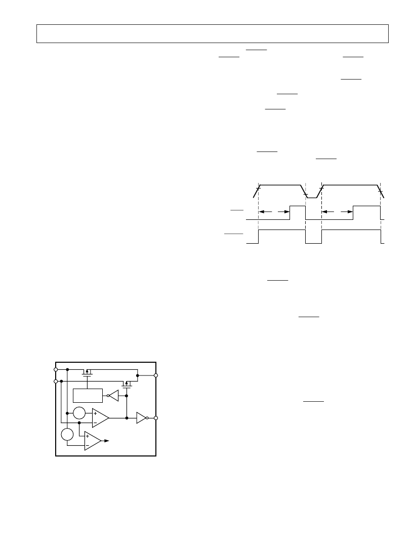
CIRCUIT INFORMAT ION
Battery Switchover Section (ADM8696)
T he battery switchover circuit is designed to switch over to
battery backup in the event of a power failure. When L L
IN
is below the reset threshold and V
CC
is below V
BAT T
, then
V
BAT T
is switched to V
OUT
.
During normal operation, with V
CC
higher than V
BAT T
, V
CC
is
internally switched to V
OUT
via an internal PMOS transistor
switch. T his switch has a typical on resistance of 0.7
and can
supply up to 100 mA at the V
OUT
terminal. V
OUT
is normally
used to drive a RAM memory bank which may require instanta-
neous currents of greater than 100 mA. If this is the case, then
a bypass capacitor should be connected to V
OUT
. T he capacitor
will provide the peak current transients to the RAM. A capaci-
tance value of 0.1
μ
F or greater may be used.
If the continuous output current requirement at V
OUT
exceeds
100 mA or if a lower V
CC
–V
OUT
voltage differential is desired,
an external PNP pass transistor may be connected in parallel
with the internal transistor. T he BAT T ON output can directly
drive the base of the external transistor.
A 7
MOSFET switch connects the V
BAT T
input to V
OUT
dur-
ing battery backup. T his MOSFET has very low input-to-out-
put differential (dropout voltage) at the low current levels
required for battery backup of CMOS RAM or other low power
CMOS circuitry. T he supply current in battery backup is typi-
cally 0.4
μ
A.
T he ADM8696 operates with battery voltages from 2.0 V to
V
CC
–0.3 V). High value capacitors, either standard electrolytic
or the farad-size double layer capacitors, can also be used for
short-term memory backup. A small charging current of typi-
cally 10 nA (0.1
μ
A max) flows out of the V
BAT T
terminal. T his
current is useful for maintaining rechargeable batteries in a fully
charged condition. T his extends the life of the backup battery
by compensating for its self-discharge current. Also note that
this current poses no problem when lithium batteries are used
for backup since the maximum charging current (0.1
μ
A) is safe
for even the smallest lithium cells.
If the battery switchover section is not used, V
BAT T
should be
connected to GND and V
OUT
should be connected to V
CC
.
V
BATT
V
CC
BATT ON
(ADM8691, ADM8693,
ADM8695, ADM8696)
V
OUT
700
mV
100
mV
GATE DRIVE
INTERNAL
SHUTDOWN SIGNAL
WHEN
V
BATT
> (V
CC
+ 0.7V)
Figure 1. Battery Switchover Schematic
相关PDF资料 |
PDF描述 |
|---|---|
| ADM8697AN | bqTINY-II Dual Input USB/AC Adpater 1-Cell Li-Ion Charger w/Timer Enable & Temp Sense, No Taper 10-SON -40 to 85 |
| ADM8697ARU | bqTINY-II Dual Input USB/AC Adpater 1-Cell Li-Ion Charger w/Timer Enable & Temp Sense, No Taper 10-SON -40 to 85 |
| ADM8697ARW | bqTINY-II Dual Input USB/AC Adpater 1-Cell Li-Ion Charger w/Charge Enable & AC Present, No Taper 10-SON -40 to 85 |
| ADM8698AN | bqTINY-II Dual Input USB/AC Adpater 1-Cell Li-Ion Charger w/Charge Enable & AC Present, No Taper 10-SON -40 to 85 |
| ADM8698ARN | bqTINY-II Dual Input USB/AC Adpater 1-Cell Li-Ion Charger w/Charge Enable & AC Present, No Taper 10-SON -40 to 85 |
相关代理商/技术参数 |
参数描述 |
|---|---|
| ADM8696ARW-REEL | 功能描述:IC SUPERVSR MPU ADJ/RESET 16SOIC RoHS:否 类别:集成电路 (IC) >> PMIC - 监控器 系列:- 标准包装:1 系列:- 类型:简单复位/加电复位 监视电压数目:1 输出:开路漏极或开路集电极 复位:高有效 复位超时:- 电压 - 阀值:1.8V 工作温度:-40°C ~ 125°C 安装类型:表面贴装 封装/外壳:6-TSOP(0.059",1.50mm 宽)5 引线 供应商设备封装:5-TSOP 包装:剪切带 (CT) 其它名称:NCP301HSN18T1GOSCT |
| ADM8696ARWZ | 功能描述:IC SUPERVSR MPU ADJ/RESET 16SOIC RoHS:是 类别:集成电路 (IC) >> PMIC - 监控器 系列:- 其它有关文件:STM6905 View All Specifications 标准包装:1 系列:- 类型:多压监控器 监视电压数目:5 输出:开路漏极或开路集电极 复位:低有效 复位超时:最小为 140 ms 电压 - 阀值:2.188V,2.955V,可调,可调,可调 工作温度:-40°C ~ 85°C 安装类型:表面贴装 封装/外壳:8-TSSOP,8-MSOP(0.118",3.00mm 宽) 供应商设备封装:8-TSSOP 包装:Digi-Reel® 产品目录页面:1197 (CN2011-ZH PDF) 其它名称:497-8728-6 |
| ADM8696ARWZ-REEL | 功能描述:IC SUPERVSR MPU ADJ/RESET 16SOIC RoHS:是 类别:集成电路 (IC) >> PMIC - 监控器 系列:- 标准包装:1 系列:- 类型:简单复位/加电复位 监视电压数目:1 输出:开路漏极或开路集电极 复位:高有效 复位超时:- 电压 - 阀值:1.8V 工作温度:-40°C ~ 125°C 安装类型:表面贴装 封装/外壳:6-TSOP(0.059",1.50mm 宽)5 引线 供应商设备封装:5-TSOP 包装:剪切带 (CT) 其它名称:NCP301HSN18T1GOSCT |
| ADM8697 | 制造商:AD 制造商全称:Analog Devices 功能描述:Microprocessor Supervisory Circuits |
| ADM8697AN | 功能描述:IC SUPERVSR MPU ADJ/RESET 16DIP RoHS:否 类别:集成电路 (IC) >> PMIC - 监控器 系列:- 标准包装:1 系列:- 类型:简单复位/加电复位 监视电压数目:1 输出:开路漏极或开路集电极 复位:高有效 复位超时:- 电压 - 阀值:1.8V 工作温度:-40°C ~ 125°C 安装类型:表面贴装 封装/外壳:6-TSOP(0.059",1.50mm 宽)5 引线 供应商设备封装:5-TSOP 包装:剪切带 (CT) 其它名称:NCP301HSN18T1GOSCT |
发布紧急采购,3分钟左右您将得到回复。