参数资料
| 型号: | ADM8832ACPZ |
| 厂商: | Analog Devices Inc |
| 文件页数: | 10/12页 |
| 文件大小: | 0K |
| 描述: | IC CHARGE PUMP REG TFT 20LFCSP |
| 标准包装: | 1 |
| 应用: | 转换器,TFT,LCD |
| 输入电压: | 2.6 V ~ 3.6 V |
| 输出数: | 3 |
| 输出电压: | -10.2V,5.1V,15.3V |
| 工作温度: | -40°C ~ 85°C |
| 安装类型: | 表面贴装 |
| 封装/外壳: | 20-LFCSP |
| 供应商设备封装: | 20-LFCSP |
| 包装: | 托盘 |
| 配用: | ADM8832EB-EVALZ-ND - BOARD EVALUATION ADM8832 REG |
�� ��
��
��ADM8832�
�THEORY� OF� OPERATION�
�SCANNING� AND� BLANKING�
�A� TFT� LCD� panel� is� made� up� of� a� bank� of� capacitors,� each�
�representing� a� pixel� in� the� display.� These� capacitors� store�
�different� levels� of� charge,� depending� on� the� amount� of�
�luminescence� required� for� a� given� pixel.� When� a� picture� is�
�displayed� on� the� panel,� a� scan� of� all� the� pixel� capacitors� is�
�performed,� placing� different� levels� of� charge� on� each� in� order� to�
�create� the� image.� The� process� of� updating� the� display� like� this� is�
�called� scanning.� Once� scanned,� an� image� is� held� by� pixel�
�capacitance,� and� the� controller� and� source� line� drivers� can� be�
�put� into� a� low� power� mode.� This� low� power� mode� is� referred� to�
�as� the� blanking� mode� on� the� ADM8832.� Over� a� finite� period� of�
�time,� this� pixel� charge� will� leak� and� the� capacitors� will� need� to�
�be� refreshed� in� order� to� maintain� the� image.�
�The� ADM8832� uses� scanning� and� blanking� modes,� as� follows.�
�When� the� TFT� LCD� panel� is� in� scanning� mode,� a� logic� high� on�
�the� SCAN/BLANK� input� places� the� device� in� high� current�
�power� mode,� providing� extra� power� (extra� current)� to� the� LCD�
�controller� and� the� source� line� drivers.� If� the� panel� continues� to�
�be� updated� (as� when� a� moving� picture� is� being� displayed),� the�
�ADM8832� can� be� continually� operated� in� scanning� mode.� If� the�
�same� image� is� kept� on� the� panel,� a� logic� low� is� applied� to� the�
�SCAN/BLANK� input,� and� the� ADM8832� enters� blanking� (low�
�current)� mode.� Depending� on� how� often� the� image� is� u� pdated,�
�TRANSIENT� RESPONSE�
�The� ADM8832� features� extremely� fast� transient� response,�
�making� it� very� suitable� for� fast� image� updates� on� TFT� LCD�
�panels.� This� means� that� even� under� changing� load� conditions�
��and� Figure� 13� show� how� the� 5.1� V� output� responds� when� a�
�maximum� load� is� dynamically� connected� and� disconnected.�
�Note� that� the� output� settles� within� 5� μs� to� less� than� 1%� of� the�
�output� level.�
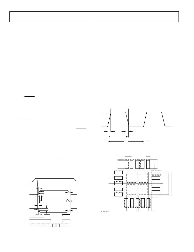
�EXTERNAL� CLOCK�
�The� ADM8832� has� an� internal� 100� kHz� oscillator,� but� an�
�external� clock� source� can� also� be� used� to� clock� the� part.� This�
�clock� source� must� be� applied� to� the� CLKIN� pin.� Power� is� saved�
�during� blanking� periods� by� disabling� the� internal� oscillator� and�
�by� switching� to� the� lower� frequency� external� clock� source.� To�
�achieve� optimum� performance� of� the� charge� pump� circuitry,� it�
�is� important� that� the� duty� cycle� of� the� external� clock� source� is�
�50%� and� that� the� rise� and� fall� times� are� less� than� 20� ns.�
�90%�
�10%�
�the� ADM8832� can� be� operated� with� a� variable� SCAN/� BLANK�
�t� R�
�t� F�
�duty� cycle.� This� helps� to� maximize� power� efficiency� and,�
�therefore,� extends� the� battery� life.�
�POWER� SEQUENCING�
�t� H�
�t� T�
�t� R� :� RISE� TIME�
�t� F� :� FALL� TIME�
�t� H�
�@� 100%� =� DUTY� CYCLE�
�t� T�
�The� gate� drive� supplies� must� be� sequenced� such� that� the� ?10� V�
�supply� is� up� before� the� +15� V� supply� for� the� TFT� panel� to� power�
�Figure� 18.� Duty� Cycle� of� External� Clock�
�on� correctly.� The� ADM8832� controls� this� sequence.� When� the�
�device� is� turned� on� (a� logic� high� on� SHDN),� the� ADM8832�
�allows� the� ?10� V� output� to� ramp� immediately,� but� holds� off� the�
�+15� V� output.� It� continues� to� do� this� until� the� negative� output�
�reaches� ?3� V.� At� this� point,� the� positive� output� is� enabled� and�
��VCC�
�SHDN�
�t� R5V�
�0.280�
�0.400�
�+5V�
�+15V�
�t� R15V�
�t� R15V�
�90%�
�10%�
�t� F5V�
�t� F15V�
�–10V�
�90%�
�10%�
�–3V�
�t� R10V�
�SOLDER� MASK�
�0.875�
�0.200�
�0.250�
�LOAD�
�SCAN/BLANK�
�EXTERNAL�
�CLOCK�
�t� F10V�
�Figure� 17.� Power� Sequence�
�Rev.� A� |� Page� 10� of� 12�
�BOARD� METALLIZATION�
�Figure� 19.� Suggested� LFCSP� 4� mm� � 4mm� 20� Lead� Land� Pattern�
�相关PDF资料 |
PDF描述 |
|---|---|
| ADM8839ACPZ-REEL7 | IC CHARGE PUMP REG TFT 20LFCSP |
| ADM9690ARNZ | IC SUPERVISOR PS/WATCHDOG 8SOIC |
| ADN2525ACPZ-REEL7 | IC LASER DRIVER 10.7GBPS 16LFCSP |
| ADN2526ACPZ-R7 | IC LASER DRIVER 11.3GBPS 16LFCSP |
| ADN2530YCPZ-500R7 | IC LASER DRVR 11.3GPBS 16LFCSP |
相关代理商/技术参数 |
参数描述 |
|---|---|
| ADM8832ACPZ1 | 制造商:AD 制造商全称:Analog Devices 功能描述:Charge Pump Regulator for Color TFT Panel |
| ADM8832ACPZ-REEL | 功能描述:IC CHARGE PUMP REG TFT 20LFCSP RoHS:是 类别:集成电路 (IC) >> PMIC - 稳压器 - 专用型 系列:- 标准包装:43 系列:- 应用:控制器,Intel VR11 输入电压:5 V ~ 12 V 输出数:1 输出电压:0.5 V ~ 1.6 V 工作温度:-40°C ~ 85°C 安装类型:表面贴装 封装/外壳:48-VFQFN 裸露焊盘 供应商设备封装:48-QFN(7x7) 包装:管件 |
| ADM8832ACPZ-REEL7 | 功能描述:IC CHARGE PUMP REG TFT 20LFCSP RoHS:是 类别:集成电路 (IC) >> PMIC - 稳压器 - 专用型 系列:- 标准包装:43 系列:- 应用:控制器,Intel VR11 输入电压:5 V ~ 12 V 输出数:1 输出电压:0.5 V ~ 1.6 V 工作温度:-40°C ~ 85°C 安装类型:表面贴装 封装/外壳:48-VFQFN 裸露焊盘 供应商设备封装:48-QFN(7x7) 包装:管件 |
| ADM8832EB-EVALZ | 功能描述:BOARD EVALUATION ADM8832 REG RoHS:是 类别:编程器,开发系统 >> 评估板 - DC/DC 与 AC/DC(离线)SMPS 系列:- 产品培训模块:Obsolescence Mitigation Program 标准包装:1 系列:True Shutdown™ 主要目的:DC/DC,步升 输出及类型:1,非隔离 功率 - 输出:- 输出电压:- 电流 - 输出:1A 输入电压:2.5 V ~ 5.5 V 稳压器拓扑结构:升压 频率 - 开关:3MHz 板类型:完全填充 已供物品:板 已用 IC / 零件:MAX8969 |
| ADM8839 | 制造商:AD 制造商全称:Analog Devices 功能描述:Charge Pump Regulator for Color TFT Panels |
发布紧急采购,3分钟左右您将得到回复。