- 您现在的位置:买卖IC网 > PDF目录9663 > ADN2814ACPZ-RL7 (Analog Devices Inc)IC CLK/DATA REC 675MBPS 32-LFCSP PDF资料下载
参数资料
| 型号: | ADN2814ACPZ-RL7 |
| 厂商: | Analog Devices Inc |
| 文件页数: | 6/28页 |
| 文件大小: | 0K |
| 描述: | IC CLK/DATA REC 675MBPS 32-LFCSP |
| 标准包装: | 1,500 |
| 类型: | 时钟和数据恢复(CDR),多路复用器 |
| PLL: | 是 |
| 主要目的: | SONET/SDH |
| 输入: | CML |
| 输出: | LVDS |
| 电路数: | 1 |
| 比率 - 输入:输出: | 1:2 |
| 差分 - 输入:输出: | 是/是 |
| 频率 - 最大: | 675MHz |
| 电源电压: | 3 V ~ 3.6 V |
| 工作温度: | -40°C ~ 85°C |
| 安装类型: | 表面贴装 |
| 封装/外壳: | 32-VFQFN 裸露焊盘,CSP |
| 供应商设备封装: | 32-LFCSP-VQ(5x5) |
| 包装: | 带卷 (TR) |
第1页第2页第3页第4页第5页当前第6页第7页第8页第9页第10页第11页第12页第13页第14页第15页第16页第17页第18页第19页第20页第21页第22页第23页第24页第25页第26页第27页第28页
ADN2814
Data Sheet
Rev. C | Page 14 of 28
THEORY OF OPERATION
The ADN2814 is a delay- and phase-locked loop circuit for
clock recovery and data retiming from an NRZ encoded data
stream. The phase of the input data signal is tracked by two
separate feedback loops, which share a common control voltage.
A high speed delay-locked loop path uses a voltage controlled
phase shifter to track the high frequency components of input
jitter. A separate phase control loop, comprised of the VCO,
tracks the low frequency components of input jitter. The initial
frequency of the VCO is set by yet a third loop that compares
the VCO frequency with the input data frequency and sets the
coarse tuning voltage. The jitter tracking phase-locked loop
controls the VCO by the fine-tuning control.
The delay and phase loops together track the phase of the input
data signal. For example, when the clock lags input data, the
phase detector drives the VCO to a higher frequency and
increases the delay through the phase shifter; both of these
actions serve to reduce the phase error between the clock and
data. The faster clock picks up phase, while the delayed data
loses phase. Because the loop filter is an integrator, the static
phase error is driven to zero.
Another view of the circuit is that the phase shifter implements
the zero required for frequency compensation of a second-order
phase-locked loop, and this zero is placed in the feedback path
and, thus, does not appear in the closed-loop transfer function.
Jitter peaking in a conventional second-order phase-locked loop
is caused by the presence of this zero in the closed-loop transfer
function. Because this circuit has no zero in the closed-loop
transfer, jitter peaking is minimized.
The delay and phase loops together simultaneously provide
wideband jitter accommodation and narrow-band jitter
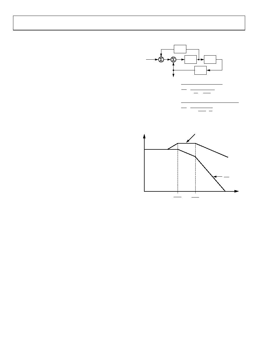
filtering. The linearized block diagram in Figure 17 shows that
the jitter transfer function, Z(s)/X(s), is a second-order low-pass
providing excellent filtering. Note that the jitter transfer has no
zero, unlike an ordinary second-order phase-locked loop. This
means that the main PLL loop has virtually zero jitter peaking
(see Figure 18). This makes this circuit ideal for signal regen-
erator applications, where jitter peaking in a cascade of
regenerators can contribute to hazardous jitter accumulation.
The error transfer, e(s)/X(s), has the same high-pass form as an
ordinary phase-locked loop. This transfer function is free to be
optimized to give excellent wideband jitter accommodation,
because the jitter transfer function, Z(s)/X(s), provides the
narrow-band jitter filtering.
X(s)
Z(s)
RECOVERED
CLOCK
e(s)
INPUT
DATA
d/sc
psh
o/s
1/n
d = PHASE DETECTOR GAIN
o = VCO GAIN
c = LOOP INTEGRATOR
psh = PHASE SHIFTER GAIN
n = DIVIDE RATIO
=
1
cn
do
s2
+
n psh
o
s+ 1
Z(s)
X(s)
JITTER TRANSFER FUNCTION
=
s2
d psh
c
s
++
do
cn
e(s)
X(s)
TRACKING ERROR TRANSFER FUNCTION
04949-017
Figure 17. ADN2814 PLL/DLL Architecture
ADN2814
Z(s)
X(s)
FREQUENCY (kHz)
JITTER PEAKING
IN ORDINARY PLL
JITTER
GAIN
(dB)
o
n psh
d psh
c
04949-
018
Figure 18. ADN2814 Jitter Response vs. Conventional PLL
The delay and phase loops contribute to overall jitter accom-
modation. At low frequencies of input jitter on the data signal,
the integrator in the loop filter provides high gain to track large
jitter amplitudes with small phase error. In this case, the VCO is
frequency modulated, and jitter is tracked as in an ordinary
phase-locked loop. The amount of low frequency jitter that can
be tracked is a function of the VCO tuning range. A wider
tuning range gives larger accommodation of low frequency
jitter. The internal loop control voltage remains small for small
phase errors; therefore, the phase shifter remains close to the
center of its range and thus contributes little to the low
frequency jitter accommodation.
相关PDF资料 |
PDF描述 |
|---|---|
| SY69753LHG TR | IC CLOCK/DATA REC 155MBPS 32TQFP |
| SY69753ALHG TR | IC CLOCK/DATA REC 125MBPS 32TQFP |
| VI-J01-MX-F2 | CONVERTER MOD DC/DC 12V 75W |
| ADN2807ACPZ-RL | IC CLOCK/DATA RECOVERY 48LFCSP |
| MS27484T24F2PA | CONN PLUG 100POS STRAIGHT W/PINS |
相关代理商/技术参数 |
参数描述 |
|---|---|
| ADN2814XCPZ | 制造商:AD 制造商全称:Analog Devices 功能描述:Continuous Rate 12.3 Mb/s to 675 Mb/s Clock and Data Recovery IC with Integrated Limiting Amp |
| ADN2815 | 制造商:AD 制造商全称:Analog Devices 功能描述:Continuous Rate 10 Mb/s to 1.25 Gb/s Clock and Data Recovery IC |
| ADN2815ACPZ | 功能描述:IC CLK/DATA REC 1.25GBPS 32LFCSP RoHS:是 类别:集成电路 (IC) >> 时钟/计时 - 专用 系列:- 标准包装:28 系列:- 类型:时钟/频率发生器 PLL:是 主要目的:Intel CPU 服务器 输入:时钟 输出:LVCMOS 电路数:1 比率 - 输入:输出:3:22 差分 - 输入:输出:无/是 频率 - 最大:400MHz 电源电压:3.135 V ~ 3.465 V 工作温度:0°C ~ 85°C 安装类型:表面贴装 封装/外壳:64-TFSOP (0.240",6.10mm 宽) 供应商设备封装:64-TSSOP 包装:管件 |
| ADN2815ACPZ-500RL7 | 功能描述:IC CLK/DATA REC 1.25GBPS 32LFCSP RoHS:是 类别:集成电路 (IC) >> 时钟/计时 - 专用 系列:- 标准包装:28 系列:- 类型:时钟/频率发生器 PLL:是 主要目的:Intel CPU 服务器 输入:时钟 输出:LVCMOS 电路数:1 比率 - 输入:输出:3:22 差分 - 输入:输出:无/是 频率 - 最大:400MHz 电源电压:3.135 V ~ 3.465 V 工作温度:0°C ~ 85°C 安装类型:表面贴装 封装/外壳:64-TFSOP (0.240",6.10mm 宽) 供应商设备封装:64-TSSOP 包装:管件 |
| ADN2815ACPZ-RL7 | 功能描述:IC CLK/DATA REC 1.25GBPS 32LFCSP RoHS:是 类别:集成电路 (IC) >> 时钟/计时 - 专用 系列:- 标准包装:28 系列:- 类型:时钟/频率发生器 PLL:是 主要目的:Intel CPU 服务器 输入:时钟 输出:LVCMOS 电路数:1 比率 - 输入:输出:3:22 差分 - 输入:输出:无/是 频率 - 最大:400MHz 电源电压:3.135 V ~ 3.465 V 工作温度:0°C ~ 85°C 安装类型:表面贴装 封装/外壳:64-TFSOP (0.240",6.10mm 宽) 供应商设备封装:64-TSSOP 包装:管件 |
发布紧急采购,3分钟左右您将得到回复。