- 您现在的位置:买卖IC网 > PDF目录1776 > ADN2841ACPZ-48 (Analog Devices Inc)IC LSR DRVR 2.7GBPS 5.5V 48LFCSP PDF资料下载
参数资料
| 型号: | ADN2841ACPZ-48 |
| 厂商: | Analog Devices Inc |
| 文件页数: | 11/16页 |
| 文件大小: | 0K |
| 描述: | IC LSR DRVR 2.7GBPS 5.5V 48LFCSP |
| 标准包装: | 1 |
| 类型: | 激光二极管驱动器(光纤) |
| 数据速率: | 2.7Gbps |
| 通道数: | 1 |
| 电源电压: | 4.5 V ~ 5.5 V |
| 电流 - 电源: | 50mA |
| 电流 - 调制: | 80mA |
| 电流 - 偏置: | 100mA |
| 工作温度: | -40°C ~ 85°C |
| 封装/外壳: | 48-VFQFN 裸露焊盘,CSP |
| 供应商设备封装: | 48-LFCSP |
| 包装: | 托盘 |
| 安装类型: | 表面贴装 |
�� �
�
�Data� Sheet�
�DATA� AND� CLOCK� INPUTS�
�Data� and� clock� inputs� are� ac-coupled� (10� nF� recommended)�
�and� terminated� via� a� 100� Ω� internal� resistor� between� the� DATAP�
�and� DATAN� pins� and� also� between� the� CLKP� and� CLKN� pins.�
�A� high� impedance� circuit� sets� the� common-mode� voltage� that�
�is� designed� to� change� over� temperature.� It� is� recommended� that�
�ac� coupling� be� used� to� eliminate� the� need� for� matching� between�
�common-mode� voltages.�
�ADN2841�
�ADN2841�
�ALARM� INTERFACES�
�A� 30� k� internal� pull-up� resistor� is� used� to� pull� the� digital� high�
�value� of� the� alarm� outputs� to� V� CC� .� However,� the� ADN2841� has� a�
�feature� that� allows� the� user� to� externally� wire� resistors� in� parallel�
�with� the� 30� k� pull-up� resistors,� thus� enabling� the� user� to� inter-�
�face� to� non-V� CC� levels.� Non-V� CC� alarm� output� levels� must� be�
��POWER� CONSUMPTION�
�The� ADN2841� die� temperature� must� be� kept� below� 125°C.� The�
�DATAP�
�DATAN�
�50?�
�TO� FLIP-FLOPS�
�50?�
�V� REG�
�R�
�R� =� 2.5k?,� DATA�
�R� =� 3k?,� CLK�
�θ� JA� is� 25°C/W� for� the� 48-lead� LFCSP� and� 32°C/W� for� the� 32-lead�
�LFCSP� when� soldered� on� a� 4-layer� board.� Both� LFCSP� packages�
�have� an� exposed� pad� and,� therefore,� must� be� soldered� to� the� PCB�
�to� achieve� this� thermal� performance.�
�T� DIE� =� T� AMBIENT� +� (� θ� JA� ×� P� )�
�I� CC� =� I� CCMIN� +� (0.3� � I� MOD� )�
�P� =� V� CC� � I� CC� +� (� I� BIAS� � V� IBIAS� )� +� (� I� MOD� � V� IMODx� )�
�400μA� TYP�
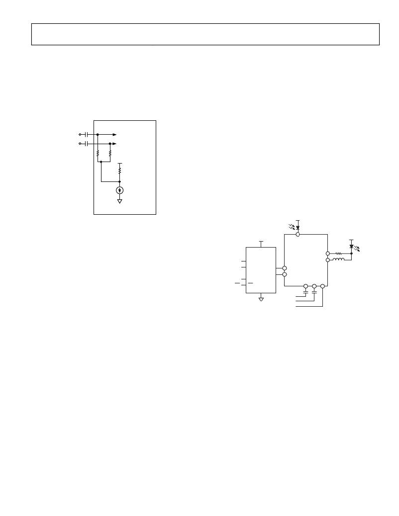
�Figure� 9.� AC� Coupling� of� Data� Inputs�
�Thus,� the� maximum� combination� of� I� BIAS� +� I� MOD� must� be�
�calculated.�
�V� CC�
�CCBIAS�
�CCBIAS� should� be� connected� to� the� IBIAS� pin� if� the� laser� diode�
�is� connected� to� the� ADN2841� using� a� capacitor.� CCBIAS� is� a�
�current� sink� to� GND.�
�Tx�
�V� CC�
�ADN2850�
�SDI�
�IMPD�
�ADN2841�
�IMODP�
�IBIAS�
�V� CC�
�AUTOMATIC� LASER� SHUTDOWN�
�The� ADN2841� ALS� pin� allows� compliance� with� ITU-T� G.958�
�(11/94),� Section� 9.7.� When� ALS� is� logic� high,� both� bias� and�
�modulation� currents� are� turned� off.�
�Rx�
�CLK�
�CS�
�SDO�
�CLK�
�CS�
�DAC1�
�DAC2�
�PSET�
�ERSET�
�DATAP�
�Correct� operation� of� ALS� can� be� confirmed� by� the� FAIL� alarm�
�being� raised� when� ALS� is� asserted.� Note� that� this� is� the� only�
�time� that� DEGRADE� will� be� low� while� FAIL� is� high.�
�DATAN�
�IDTONE�
�Figure� 10.� Application� Using� Optical� Supervisor� ADN2850� as� a� Dual,� 10-Bit�
�Digital� Potentiometer� Using� Thin� Film� Resistor� Technology� to� Give� Very� Low�
�Temperature� Coefficients�
�Rev.� B� |� Page� 11� of� 16�
�相关PDF资料 |
PDF描述 |
|---|---|
| ADN2847ACPZ-32 | IC LSR DRVR 3.3GBPS 3.6V 32LFCSP |
| ADN2848ACPZ-32-RL7 | IC LASER DRIVER 1.25GBPS 32LFCSP |
| ADN2870ACPZ-RL7 | IC LSR DRVR 3.3GPBS 3.6V 24LFCSP |
| ADN2871ACPZ-RL7 | IC LASER DRIVER 4.25GBPS 24LFCSP |
| ADN2872ACPZ-R7 | IC LASR DVR 3.3GBPS 3.3V 24LFCSP |
相关代理商/技术参数 |
参数描述 |
|---|---|
| ADN2841ACPZ-48-RL | 功能描述:IC LSR DRVR 2.7GBPS 5.5V 48LFCSP RoHS:是 类别:集成电路 (IC) >> PMIC - 激光驱动器 系列:- 产品培训模块:Lead (SnPb) Finish for COTS Obsolescence Mitigation Program 标准包装:60 系列:- 类型:激光二极管驱动器 数据速率:- 通道数:4 电源电压:3.3V 电流 - 电源:- 电流 - 调制:- 电流 - 偏置:- 工作温度:0°C ~ 70°C 封装/外壳:40-TQFN 裸露焊盘 供应商设备封装:40-TQFN EP 包装:托盘 安装类型:表面贴装 |
| ADN2843 | 制造商:AD 制造商全称:Analog Devices 功能描述:10.709 Gbps Laser Diode Driver Chipset |
| ADN2843CHIPSET | 制造商:Analog Devices 功能描述:Drivers, 10.709Gbps Laser Diode Driver Chipset |
| ADN2843CHIPSET-B | 制造商:Analog Devices 功能描述:Drivers, 10.709Gbps Laser Diode Driver Chipset |
| ADN2844BCP-32 | 制造商:Analog Devices 功能描述: |
发布紧急采购,3分钟左右您将得到回复。