- 您现在的位置:买卖IC网 > PDF目录1899 > ADN4604ASVZ-RL (Analog Devices Inc)IC CROSSPOINT SWIT 16X16 100TQFP PDF资料下载
参数资料
| 型号: | ADN4604ASVZ-RL |
| 厂商: | Analog Devices Inc |
| 文件页数: | 14/40页 |
| 文件大小: | 0K |
| 描述: | IC CROSSPOINT SWIT 16X16 100TQFP |
| 标准包装: | 1,000 |
| 系列: | XStream™ |
| 功能: | 交叉点开关 |
| 电路: | 1 x 16:16 |
| 电压电源: | 单电源 |
| 电压 - 电源,单路/双路(±): | 2.7 V ~ 3.6 V |
| 电流 - 电源: | 95mA |
| 工作温度: | -40°C ~ 85°C |
| 安装类型: | 表面贴装 |
| 封装/外壳: | 100-TQFP 裸露焊盘 |
| 供应商设备封装: | 100-TQFP-EP(14x14) |
| 包装: | 带卷 (TR) |
第1页第2页第3页第4页第5页第6页第7页第8页第9页第10页第11页第12页第13页当前第14页第15页第16页第17页第18页第19页第20页第21页第22页第23页第24页第25页第26页第27页第28页第29页第30页第31页第32页第33页第34页第35页第36页第37页第38页第39页第40页
Data Sheet
ADN4604
Rev. A | Page 21 of 40
Advanced Settings
In addition to the basic settings provided in the TX basic
control registers, advanced settings are available in TX Drive 0
Control and TX Drive 1 Control registers (Address 0x30 to
Address 0x4F). The advanced settings are useful in applications
where each output requires an individually programmed
preemphasis or output level setting beyond what is available
in the lookup table in basic mode. To enable these advanced
settings, set the TX CTL SELECT bit in the TX basic control
register to a logic high. Next, program the TX Drive 0 control
and Drive 1 control registers (Address 0x30 to Address 0x4F) to
the desired output level and boost values. A subset of possible
settings is provided in Table 13. An expanded list of available
settings is shown in Table 19 in the Applications Information
section. These advanced settings can also be used to modify the
TX lookup table settings (Address 0x60 to Address 0x6F). The
advanced settings register map is shown in Table 15.
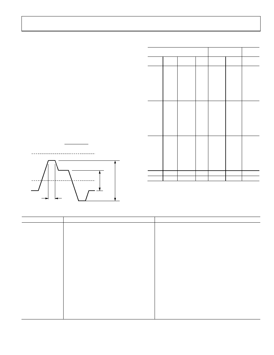
The preemphasis boost equation follows.
)
1
(
log
20
]
dB
[
10
V
DC
SW
DC
SW
PE
SW
Gain
(1)
VTTO
VH-PE
VSW-PE
VL-PE
VL-DC
VSW-DC
VH-DC
VOCM
TPE
0
793
4-
0
44
Figure 44. Signal Level Definitions
Table 13. TX Preemphasis and Output Swing Advanced
Settings
Single-Ended Output Levels and
PE Boost
Register
Settings
Output
Current
(mV)
VSW-PE1
(mV)
PE Boost
%
PE
(dB)
TX
Drive 0
TX
Drive 1
ITTO1 (mA)
200
0.00
0xBB
0x00
8
200
300
50.00
3.52
0xBB
0x99
12
200
350
75.00
4.86
0xBB
0xAA
14
200
400
100.00
6.02
0xBB
16
200
450
125.00
7.04
0xBB
0xCC
18
200
500
150.00
7.96
0xBB
0xDD
20
200
600
200.00
9.54
0xBB
0xFF
24
300
0.00
0xDD
0x00
12
300
400
33.33
2.50
0xDD
0x99
16
300
450
50.00
3.52
0xDD
0xAA
18
300
500
66.67
4.44
0xDD
0xBB
20
300
550
83.33
5.26
0xDD
0xCC
22
300
600
100.00
6.02
0xDD
24
300
700
133.33
7.36
0xDD
0xFF
28
400
0.00
0xFF
0x00
16
400
500
25.00
1.94
0xFF
0x99
20
400
550
37.50
2.77
0xFF
0xAA
22
400
600
50.00
3.52
0xFF
0xBB
24
400
650
62.50
4.22
0xFF
0xCC
26
400
700
75.00
4.86
0xFF
0xDD
28
400
800
100.00
6.02
0xFF
32
500
0.00
0xFF
0x0B
20
600
0.00
0xFF
0x0F
24
1 Symbol definitions are shown in Table 14.
Table 14. Symbol Definitions
Symbol
Formula
Definition
IDC
Programmable
Output current that sets output level
IPE
Programmable
Output current for PE delayed tap
ITTO
IDC + IPE
Total transmitter output current
TPE
Preemphasis pulse width
VDPP-DC
25 Ω × IDC × 2
Peak-to-peak differential voltage swing of non-
preemphasized waveform
VDPP-PE
25 Ω × ITTO × 2
Peak-to-peak differential voltage swing of preemphasized
waveform
VSW-DC
VDPP-DC/2 = VH-DC – VL-DC
DC single-ended voltage swing
VSW-PE
VDPP-PE/2 = VH-PE – VL-PE
Preemphasized single-ended voltage swing
VOCM_DC-COUPLED
25 Ω × ITTO/2
Output common-mode shift, dc-coupled outputs
VOCM_AC-COUPLED
50 Ω × ITTO/2
Output common-mode shift, ac-coupled outputs
VOCM
VTTO VOCM = ( VH-DC + VL-DC )/2
Output common-mode voltage
VH-DC
VTTO VOCM + VDPP-DC/2
DC single-ended output high voltage
VL-DC
VTTO VOCM VDPP-DC/2
DC single-ended output low voltage
VH-PE
VTTO VOCM + VDPP-PE/2
Maximum single-ended output voltage
VL-PE
VTTO VOCM VDPP-PE/2
Minimum single-ended output voltage
VTTO
Output termination voltage
相关PDF资料 |
PDF描述 |
|---|---|
| ADN4605ABPZ | IC CROSSPOINT SWITCH 352BGA |
| ADN4661BRZ-REEL7 | IC DRIVER DIFF LVDS 1CH 8SOIC |
| ADN4662BRZ-REEL7 | IC RCVR DIFF LVDS 1CH 8SOIC |
| ADN4663BRZ-REEL7 | IC DRIVER DIFF LVDS 2CH 8SOIC |
| ADN4664BRZ-REEL7 | IC RCVR DIFF LVDS 2CH 8SOIC |
相关代理商/技术参数 |
参数描述 |
|---|---|
| ADN4604-EVALZ | 制造商:Analog Devices 功能描述:EVALUATION BOARD - Boxed Product (Development Kits) |
| ADN4604XSVZ | 制造商:Analog Devices 功能描述:4.25GBPS 16X16 CROSSBAR SWITCH - Trays |
| ADN4605 | 制造商:AD 制造商全称:Analog Devices 功能描述:4.25 Gbps 40 × 40 Digital Crosspoint Switch 3 dB, 6 dB, or 12 dB boost |
| ADN4605_1111 | 制造商:AD 制造商全称:Analog Devices 功能描述:4.25 Gbps 40 ?? 40 Digital |
| ADN4605ABPZ | 功能描述:IC CROSSPOINT SWITCH 352BGA RoHS:是 类别:集成电路 (IC) >> 接口 - 模拟开关,多路复用器,多路分解器 系列:XStream™ 应用说明:Ultrasound Imaging Systems Application Note 产品培训模块:Lead (SnPb) Finish for COTS Obsolescence Mitigation Program 标准包装:250 系列:- 功能:开关 电路:单刀单掷 导通状态电阻:48 欧姆 电压电源:单电源 电压 - 电源,单路/双路(±):2.7 V ~ 5.5 V 电流 - 电源:5µA 工作温度:0°C ~ 70°C 安装类型:表面贴装 封装/外壳:48-LQFP 供应商设备封装:48-LQFP(7x7) 包装:托盘 |
发布紧急采购,3分钟左右您将得到回复。