- 您现在的位置:买卖IC网 > PDF目录10195 > ADN4696EBRZ-RL7 (Analog Devices Inc)IC TXRX LVDS 2CH 8SOIC PDF资料下载
参数资料
| 型号: | ADN4696EBRZ-RL7 |
| 厂商: | Analog Devices Inc |
| 文件页数: | 1/20页 |
| 文件大小: | 0K |
| 描述: | IC TXRX LVDS 2CH 8SOIC |
| 标准包装: | 1,000 |
| 系列: | * |
3.3 V, 200 Mbps, Half- and Full-Duplex,
High Speed M-LVDS Transceivers
Data Sheet
Rev.
0
Information furnished by Analog Devices is believed to be accurate and reliable. However, no
responsibilityisassumedbyAnalogDevicesforitsuse,norforanyinfringementsofpatentsorother
rightsofthirdpartiesthatmayresultfromitsuse.Specificationssubjecttochangewithoutnotice.No
license is granted by implication or otherwise under any patent or patent rights of Analog Devices.
Trademarksandregisteredtrademarksarethepropertyoftheirrespectiveowners.
One Technology Way, P.O. Box 9106, Norwood, MA 02062-9106, U.S.A.
Tel: 781.329.4700
Fax: 781.461.3113
2011 Analog Devices, Inc. All rights reserved.
FEATURES
Multipoint LVDS transceivers (low voltage differential
signalling driver and receiver pairs)
200 Mbps (100 MHz) switching rates
Supporting bus loads of 30 to 55
Receiver type:
Type 2 (ADN4696E/ADN4697E): threshold offset of 100 mV
for open-circuit and bus-idle fail-safe
Conforms to TIA/EIA-899 standard for M-LVDS
Glitch-free power-up/power-down on M-LVDS bus
Controlled transition times on driver output
Common-mode range: 1 V to +3.4 V, allowing
communication with 2 V of ground noise
Driver outputs high-Z when disabled or powered off
Enhanced ESD protection on bus pins
±15 kV HBM (human body model), air discharge
±8 kV HBM (human body model), contact discharge
±10 kV IEC 61000-4-2, air discharge
±8 kV IEC 61000-4-2, contact discharge
Operating temperature range of 40°C to +85°C
Available packages
8-lead SOIC (ADN4696E)
14-lead SOIC (ADN4697E)
APPLICATIONS
Backplane and cable multipoint data transmission
Multipoint clock distribution
Low power, high speed alternative to shorter RS-485 links
Networking routers and switches
Wireless base station infrastructure
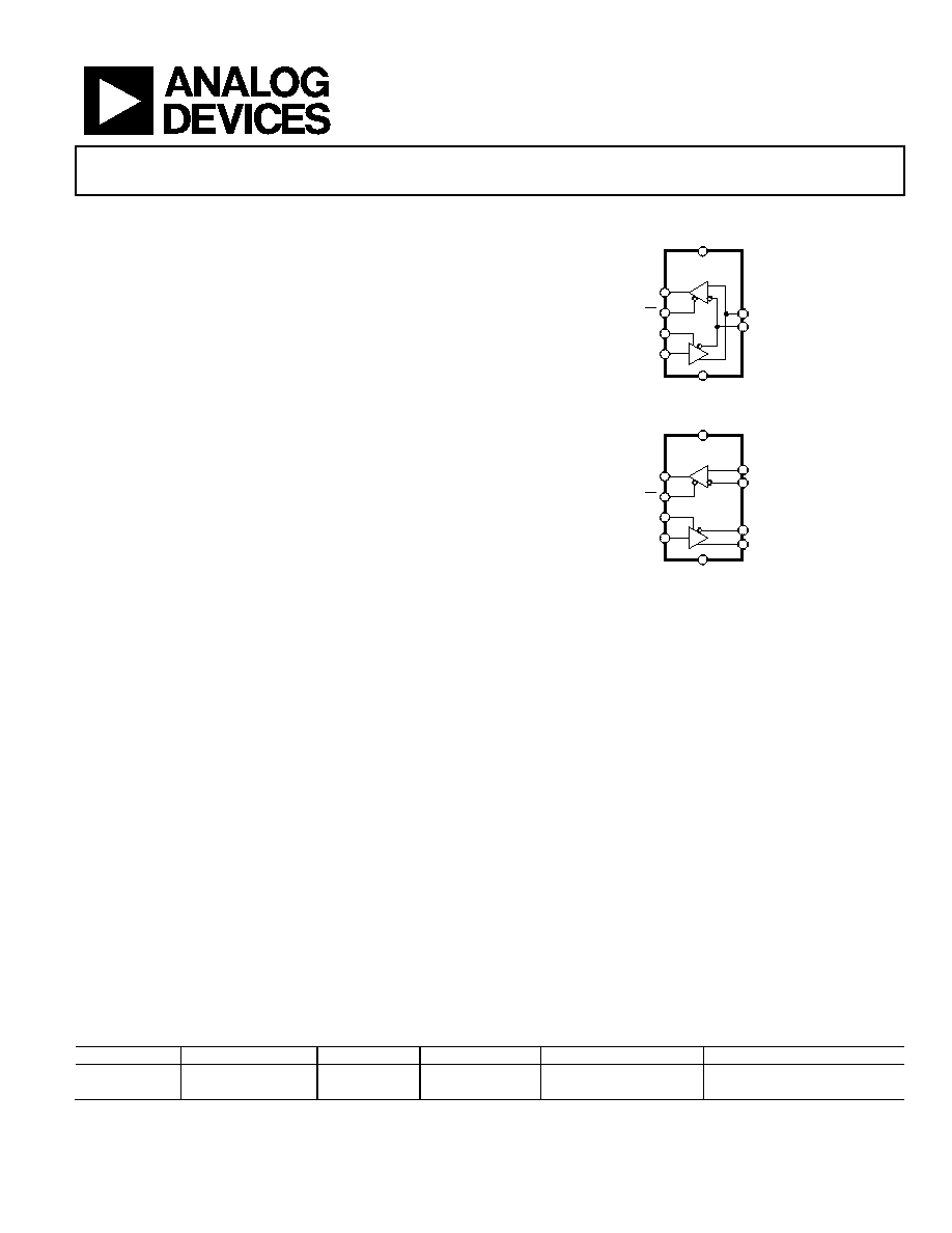
FUNCTIONAL BLOCK DIAGRAMS
ADN4696E
VCC
GND
RO
R
D
RE
DE
A
B
DI
10355-
001
Figure 1.
ADN4697E
VCC
GND
RO
R
D
RE
DE
DI
10355-
002
A
B
Z
Y
Figure 2.
GENERAL DESCRIPTION
The ADN4696E/ADN4697E are multipoint low voltage
differential signalling (M-LVDS) transceivers (driver and
receiver pairs) that can operate at up to 200 Mbps (100 MHz).
The receivers detect the bus state with a differential input of as
little as 50 mV over a common-mode voltage range of 1 V to
+3.4 V. ESD protection of up to ±15 kV is implemented on the
bus pins.
The parts adhere to the TIA/EIA-899 standard for M-LVDS and
are similar to counterpart LVDS devices that comply with the
TIA/EIA-644 standard for LVDS but designed with features for
multipoint applications. These features include a driver output
that supports multipoint bus loads as low as 30 , with controlled
transition times to permit stubs from the backbone transmission
line. Up to 32 nodes can be connected to the bus.
The ADN4696E/ADN4697E are Type 2 receivers exhibiting an
offset threshold, guaranteeing the output state when the bus is idle
(bus-idle fail-safe) or the inputs are open (open-circuit fail-safe).
The ADN4696E/ADN4697E are available as half-duplex
configurations in an 8-lead SOIC package (ADN4696E)
or as full-duplex configurations in a 14-lead SOIC package
(ADN4697E). A part selection table for ADN469xE parts is
shown in Table 1.
Table 1. ADN469xE Selection Table
Part No.
Receiver Type
Data Rate
Package
Half-/Full-Duplex
Evaluation Board
Type 2
200 Mbps
8-lead SOIC
Half
EVAL-ADN469xEHDEBZ
Type 2
200 Mbps
14-lead SOIC
Full
EVAL-ADN469xEFDEBZ
相关PDF资料 |
PDF描述 |
|---|---|
| ADN4697EBRZ-RL7 | IC TXRX LVDS 2CH 14SOIC |
| ADM1490EBRZ-REEL7 | IC TXRX RS485 FULL DUPLEX 8SOIC |
| VE-2ND-CU-F4 | CONVERTER MOD DC/DC 85V 200W |
| VE-JWP-MX-S | CONVERTER MOD DC/DC 13.8V 75W |
| VE-23J-MX-F3 | CONVERTER MOD DC/DC 36V 75W |
相关代理商/技术参数 |
参数描述 |
|---|---|
| ADN4697E | 制造商:AD 制造商全称:Analog Devices 功能描述:3.3 V, 100 Mbps, Half- and Full-Duplex |
| ADN4697EBRZ | 功能描述:IC RCVR LVDS 2CH 14SOIC RoHS:是 类别:集成电路 (IC) >> 接口 - 驱动器,接收器,收发器 系列:* 标准包装:27 系列:- 类型:收发器 驱动器/接收器数:3/3 规程:RS232,RS485 电源电压:4.75 V ~ 5.25 V 安装类型:表面贴装 封装/外壳:28-SOIC(0.295",7.50mm 宽) 供应商设备封装:28-SOIC 包装:管件 |
| ADN4697EBRZ-RL7 | 功能描述:IC TXRX LVDS 2CH 14SOIC RoHS:是 类别:集成电路 (IC) >> 接口 - 驱动器,接收器,收发器 系列:* 标准包装:121 系列:- 类型:收发器 驱动器/接收器数:1/1 规程:RS422,RS485 电源电压:3 V ~ 3.6 V 安装类型:表面贴装 封装/外壳:10-WFDFN 裸露焊盘 供应商设备封装:10-DFN(3x3) 包装:管件 |
| ADN5-24-1PM | 制造商:Johnson Components 功能描述:AC/DC Power Supply Single-OUT 24V 5A 120W 制造商:Emerson Network Power - Embedded Power 功能描述:PSU DIN RAIL 24V 5A 制造商:EMERSON NETWORK POWER 功能描述:PSU, DIN RAIL, 24V, 5A |
| ADN5-24-1PM-C | 功能描述:DIN导轨式电源 120W 24V @5A 1-Phase Metal - C Series RoHS:否 制造商:Mean Well 产品:Linear Supplies 商用/医用:Commercial 输出功率额定值:960 W 输入电压:180 VAC to 264 VAC, 254 VDC to 370 VDC 输出端数量:1 输出电压(通道 1):48 V 输出电流(通道 1): 输出电压(通道 2): 输出电流(通道 2): 输出电压(通道 3): 输出电流(通道 3): 尺寸:150 mm L x 110 mm W |
发布紧急采购,3分钟左右您将得到回复。