参数资料
| 型号: | ADP122AUJZ-2.9-R7 |
| 厂商: | Analog Devices Inc |
| 文件页数: | 13/24页 |
| 文件大小: | 0K |
| 描述: | IC REG LDO 2.9V .3A 5TSOT |
| 标准包装: | 1 |
| 稳压器拓扑结构: | 正,固定式 |
| 输出电压: | 2.9V |
| 输入电压: | 最高 5.5V |
| 电压 - 压降(标准): | 0.085V @ 300mA |
| 稳压器数量: | 1 |
| 电流 - 输出: | 300mA(最小值) |
| 电流 - 限制(最小): | 350mA |
| 工作温度: | -40°C ~ 85°C |
| 安装类型: | 表面贴装 |
| 封装/外壳: | SOT-23-5 细型,TSOT-23-5 |
| 供应商设备封装: | TSOT-23-5 |
| 包装: | 标准包装 |
| 产品目录页面: | 792 (CN2011-ZH PDF) |
| 其它名称: | ADP122AUJZ-2.9-R7DKR |
�� �
�
�Data� Sheet�
�Therefore,� the� capacitor� chosen� in� this� example� meets� the�
�minimum� capacitance� requirement� of� the� LDO� over� tem-�
�perature� and� tolerance� at� the� chosen� output� voltage.�
�1.1�
�1.0�
�ADP122/ADP123�
�To� guarantee� the� performance� of� the� ADP122/ADP123,� it� is�
�imperative� that� the� effects� of� dc� bias,� temperature,� and� tolerances�
�0.9�
�RISING�
�on� the� behavior� of� the� capacitors� are� evaluated� for� each� application.�
�UNDERVOLTAGE� LOCKOUT�
�The� ADP122/ADP123� have� an� internal� undervoltage� lockout�
�circuit� that� disables� all� inputs� and� the� output� when� the� input�
�voltage� is� less� than� approximately� 2� V.� This� ensures� that� the�
�0.8�
�0.7�
�0.6�
�FALLING�
�ADP122/ADP123� inputs� and� the� output� behave� in� a� predictable�
�manner� during� power-up.�
�0.5�
�2.2�
�2.7�
�3.2�
�3.7�
�4.2�
�4.7�
�5.2�
�ENABLE� FEATURE�
�The� ADP122/ADP123� uses� the� EN� pin� to� enable� and� disable� the�
�VOUT� pin� under� normal� operating� conditions.� As� shown� in�
��VOUT� turns� on.� Conversely,� when� a� falling� voltage� on� EN� crosses�
�the� inactive� threshold,� VOUT� turns� off.�
�3.5�
�3.0�
�2.5�
�2.0�
�V� IN� (V)�
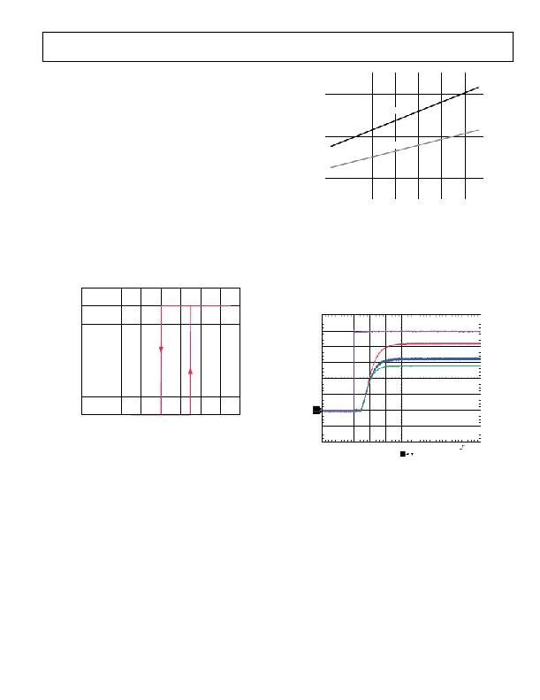
�Figure� 36.� Typical� EN� Pin� Thresholds� vs.� Input� Voltage�
�The� ADP122/ADP123� utilize� an� internal� soft� start� to� limit� the�
�in-rush� current� when� the� output� is� enabled.� The� start-up� time�
�for� the� 2.8� V� option� is� approximately� 350� μs� from� the� time� the�
�EN� active� threshold� is� crossed� to� when� the� output� reaches� 90%�
�of� its� final� value.� As� shown� in� Figure� 37,� the� start-up� time� is�
�dependent� on� the� output� voltage� setting� and� increases� slightly�
�as� the� output� voltage� increases.�
�V� IN� =� 5V�
�V� OUT� =� 4.2V�
�V� OUT� =� 3.3V�
�1.5�
�V� OUT� =� 2.8V�
�1.0�
�0.5�
�0�
�1�
�2�
�0�
�0.2�
�0.4�
�0.6�
�0.8�
�1.0�
�1.2�
�1.4�
�1.6�
�V� EN�
�Figure� 35.� Typical� EN� Pin� Operation�
�As� shown� in� Figure� 35,� the� EN� pin� has� built-in� hysteresis.� This�
�CH1� 1.00V�
�CH2� 1.00V�
�M200μs�
�T� 600.000μs�
�A� CH1�
�3.08V�
�prevents� on/off� oscillations� that� may� occur� due� to� noise� on� the�
�EN� pin� as� it� passes� through� the� threshold� points.�
�The� active� and� inactive� thresholds� of� the� EN� pin� are� derived� from�
�the� VIN� voltage.� Therefore,� these� thresholds� vary� as� the� input�
�voltage� changes.� Figure� 36� shows� typical� EN� active� and� inactive�
�thresholds� when� the� VIN� voltage� varies� from� 2.3� V� to� 5.5� V.�
�Rev.� E� |� Page� 13� of� 24�
�Figure� 37.� Typical� Start-Up� Time�
�相关PDF资料 |
PDF描述 |
|---|---|
| ADP124ARHZ-2.85-R7 | IC REG LDO 2.85V .5A 8MSOP |
| ADP130AUJZ-2.5-R7 | IC REG LDO 2.5V .35A TSOT-23-5 |
| ADP150AUJZ-2.5-R7 | IC REG LDO 2.5V .15A TSOT-5 |
| ADP151ACPZ-3.0-R7 | IC REG LDO 3V .2A 6LFCSP |
| ADP160AUJZ-1.5-R7 | IC REG LDO 1.5V .15A 5TSOT |
相关代理商/技术参数 |
参数描述 |
|---|---|
| ADP122AUJZ-3.0-R7 | 功能描述:IC REG LDO 3V .3A 5TSOT RoHS:是 类别:集成电路 (IC) >> PMIC - 稳压器 - 线性 系列:- 标准包装:3,000 系列:- 稳压器拓扑结构:正,固定式 输出电压:3V 输入电压:最高 5.5V 电压 - 压降(标准):0.12V @ 150mA 稳压器数量:1 电流 - 输出:150mA(最小值) 电流 - 限制(最小):220mA 工作温度:-40°C ~ 125°C 安装类型:表面贴装 封装/外壳:SOT-23-5 细型,TSOT-23-5 供应商设备封装:TSOT-23-5 包装:带卷 (TR) 其它名称:ADP160AUJZ-3.0-R7TR |
| ADP122AUJZ-3.3-R7 | 功能描述:IC REG LDO 3.3V .3A 5TSOT RoHS:是 类别:集成电路 (IC) >> PMIC - 稳压器 - 线性 系列:- 标准包装:3,000 系列:- 稳压器拓扑结构:正,固定式 输出电压:3V 输入电压:最高 5.5V 电压 - 压降(标准):0.12V @ 150mA 稳压器数量:1 电流 - 输出:150mA(最小值) 电流 - 限制(最小):220mA 工作温度:-40°C ~ 125°C 安装类型:表面贴装 封装/外壳:SOT-23-5 细型,TSOT-23-5 供应商设备封装:TSOT-23-5 包装:带卷 (TR) 其它名称:ADP160AUJZ-3.0-R7TR |
| ADP122AUJZ-3.3-R7 | 制造商:Analog Devices 功能描述:IC LDO VOLT REG 3.3V 0.3A TSOT-5 制造商:Analog Devices 功能描述:IC, LDO VOLT REG, 3.3V, 0.3A, TSOT-5 |
| ADP122-BL1-EVZ | 制造商:Analog Devices 功能描述:BLANK ADISIMPOWER EVAL ADP122 - Boxed Product (Development Kits) |
| ADP122UJZ-REDYKIT | 功能描述:KIT REDI TOOL 2.5/3.3 ADP123 RoHS:是 类别:编程器,开发系统 >> 评估板 - 线性稳压器 (LDO) 系列:Redykit™ 产品变化通告:1Q2012 Discontinuation 30/Mar/2012 设计资源:NCP590MNDPTAGEVB Gerber Files 标准包装:1 系列:- 每 IC 通道数:2 - 双 输出电压:1.8V,2.8V 电流 - 输出:300mA 输入电压:2.1 ~ 5.5 V 稳压器类型:正,固定式 工作温度:-40°C ~ 85°C 板类型:完全填充 已供物品:板 已用 IC / 零件:NCP590MNDP 其它名称:NCP590MNDPTAGEVB-NDNCP590MNDPTAGEVBOS |
发布紧急采购,3分钟左右您将得到回复。