- 您现在的位置:买卖IC网 > PDF目录16947 > ADP1752-1.5-EVALZ (Analog Devices Inc)BOARD EVAL AD1752 1.5V PDF资料下载
参数资料
| 型号: | ADP1752-1.5-EVALZ |
| 厂商: | Analog Devices Inc |
| 文件页数: | 12/20页 |
| 文件大小: | 0K |
| 描述: | BOARD EVAL AD1752 1.5V |
| 标准包装: | 1 |
| 每 IC 通道数: | 1 - 单 |
| 输出电压: | 1.5V |
| 电流 - 输出: | 800mA |
| 输入电压: | 1.6 ~ 3.6 V |
| 稳压器类型: | 正,固定式 |
| 工作温度: | -40°C ~ 125°C |
| 板类型: | 完全填充 |
| 已供物品: | 板 |
| 已用 IC / 零件: | ADP1752-1.5 |
�� �
�
�ADP1752/ADP1753�
�Data� Sheet�
�1�
�T�
�EN�
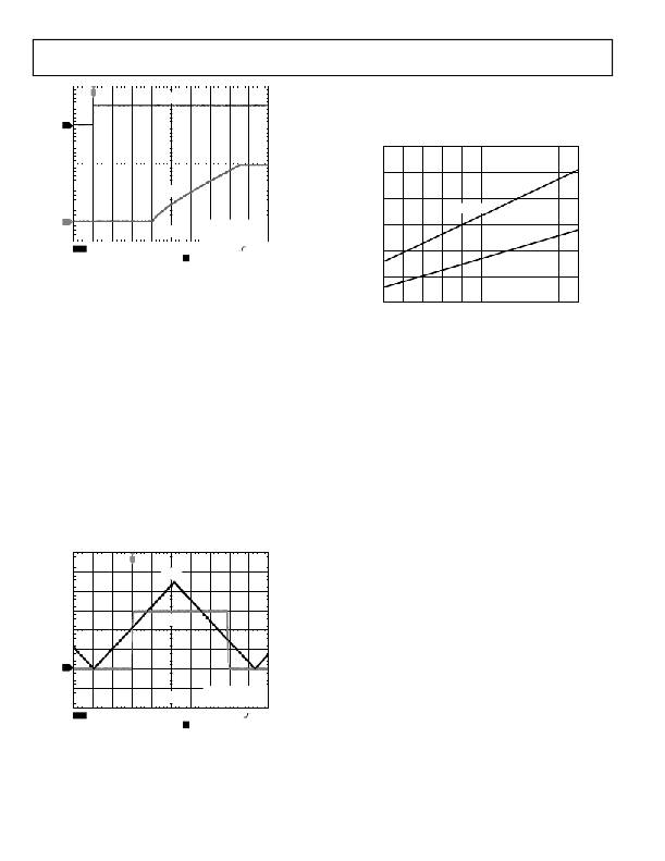
�The� EN� pin� active/inactive� thresholds� are� derived� from� the� VIN�
�voltage.� Therefore,� these� thresholds� vary� with� changing� input�
�voltage.� Figure� 29� shows� typical� EN� active/inactive� thresholds�
�when� the� input� voltage� varies� from� 1.6� V� to� 3.6� V.�
�1.1�
�1.0�
�V� OUT�
�0.9�
�EN� ACTIVE�
�2�
�500mV/DIV�
�V� OUT� =� 1.5V�
�C� IN� =� C� OUT� =� 4.7μF�
�0.8�
�EN� INACTIVE�
�CH1� 2.0V� BW�
�CH2� 500mV� BW� M40μs�
�A� CH1�
�920mV�
�0.7�
�T� 9.8%�
�Figure� 27.� V� OUT� Ramp-Up� with� Internal� Soft� Start�
��0.6�
�The� output� voltage� of� the� ADP1753� can� be� set� over� a� 0.75� V� to�
�0.5�
�1.6�
�1.8�
�2.0�
�2.2�
�2.4�
�2.6�
�2.8�
�3.0�
�3.2�
�3.4�
�3.6�
�3.3� V� range.� The� output� voltage� is� set� by� connecting� a� resistive�
�voltage� divider� from� VOUT� to� ADJ.� The� output� voltage� is� calcu-�
�lated� using� the� following� equation:�
�INPUT� VOLTAGE� (V)�
�Figure� 29.� Typical� EN� Pin� Thresholds� vs.� Input� Voltage�
�POWER-GOOD� FEATURE�
�V� OUT� =� 0.5� V� � (1� +� R1� /� R2� )�
�(2)�
�The� ADP1752� /� ADP1753� provide� a� power-good� pin,� PG,� to�
�where:�
�R1� is� the� resistor� from� VOUT� to� ADJ.�
�R2� is� the� resistor� from� ADJ� to� GND.�
�The� maximum� bias� current� into� ADJ� is� 150� nA.� Therefore,� to�
�achieve� less� than� 0.5%� error� due� to� the� bias� current,� use� values�
�less� than� 60� k� for� R2.�
�ENABLE� FEATURE�
�The� ADP1752� /� ADP1753� use� the� EN� pin� to� enable� and� disable�
�the� VOUT� pin� under� normal� operating� conditions.� As� shown� in�
��threshold,� VOUT� turns� on.� When� a� falling� voltage� on� EN�
�crosses� the� inactive� threshold,� VOUT� turns� off.�
�indicate� the� status� of� the� output.� This� open-drain� output�
�requires� an� external� pull-up� resistor� to� V� IN� .� If� the� part� is� in�
�shutdown,� in� current� limit� mode,� in� thermal� shutdown,� or� if� it�
�falls� below� 90%� of� the� nominal� output� voltage,� PG� immediately�
�transitions� low.� During� soft� start,� the� rising� threshold� of� the�
�power-good� signal� is� 93.5%� of� the� nominal� output� voltage.�
��have� sufficient� input� voltage� to� turn� on� the� internal� PG� transistor.�
�An� optional� soft� start� delay� can� be� detected.� The� PG� transistor�
�is� terminated� via� a� pull-up� resistor� to� V� OUT� or� V� IN� .�
�Power-good� accuracy� is� 93.5%� of� the� nominal� regulator� output�
�voltage� when� this� voltage� is� rising,� with� a� 90%� trip� point� when�
�this� voltage� is� falling.�
�T�
�EN�
�Regulator� input� voltage� brownouts� or� glitches� trigger� a� power�
�no-good� if� V� OUT� falls� below� 90%.�
�A� normal� power-down� triggers� a� power� no-good� when� V� OUT�
�drops� below� 90%.�
�V� OUT�
�1� 2�
�500mV/DIV�
�V� OUT� =� 1.5V�
�C� IN� =� C� OUT� =� 4.7μF�
�CH1� 500mV� BW� CH2� 500mV� BW� M2.0ms�
�A� CH1�
�1.05V�
�T� 29.6%�
�Figure� 28.� Typical� EN� Pin� Operation�
�As� shown� in� Figure� 28,� the� EN� pin� has� hysteresis� built� in.� This�
�hysteresis� prevents� on/off� oscillations� that� can� occur� due� to�
�noise� on� the� EN� pin� as� it� passes� through� the� threshold� points.�
�Rev.� F� |� Page� 12� of� 20�
�相关PDF资料 |
PDF描述 |
|---|---|
| 0982660988 | CBL 29POS 0.5MM JMPR TYPE D 2" |
| ADP121CB-3.3-EVALZ | BOARD EVAL ADP121-1 3.3V OUTPUT |
| EYM18DTMH-S189 | CONN EDGECARD 36POS R/A .156 SLD |
| 814554-000 | BOOT MOLDED |
| 234A132-25-0 | BOOT MOLDED |
相关代理商/技术参数 |
参数描述 |
|---|---|
| ADP1752ACPZ-0.75R7 | 功能描述:IC REG LDO 0.75V .8A 16LFCSP RoHS:是 类别:集成电路 (IC) >> PMIC - 稳压器 - 线性 系列:- 标准包装:1 系列:- 稳压器拓扑结构:正,固定式 输出电压:3.3V 输入电压:2.5 V ~ 5.5 V 电压 - 压降(标准):0.1V @ 200mA 稳压器数量:2 电流 - 输出:300mA 电流 - 限制(最小):350mA 工作温度:-40°C ~ 85°C 安装类型:表面贴装 封装/外壳:8-UFQFN 供应商设备封装:8-MLPQ-UT(1.5x1.5) 包装:剪切带 (CT) 产品目录页面:1358 (CN2011-ZH PDF) 其它名称:SC560HULCT |
| ADP1752ACPZ-1.0-R7 | 功能描述:IC REG LDO 1V .8A 16LFCSP RoHS:是 类别:集成电路 (IC) >> PMIC - 稳压器 - 线性 系列:- 标准包装:1 系列:- 稳压器拓扑结构:正,固定式 输出电压:3.3V 输入电压:2.5 V ~ 5.5 V 电压 - 压降(标准):0.1V @ 200mA 稳压器数量:2 电流 - 输出:300mA 电流 - 限制(最小):350mA 工作温度:-40°C ~ 85°C 安装类型:表面贴装 封装/外壳:8-UFQFN 供应商设备封装:8-MLPQ-UT(1.5x1.5) 包装:剪切带 (CT) 产品目录页面:1358 (CN2011-ZH PDF) 其它名称:SC560HULCT |
| ADP1752ACPZ-1.1-R7 | 功能描述:IC REG LDO 1.1V .8A 16LFCSP RoHS:是 类别:集成电路 (IC) >> PMIC - 稳压器 - 线性 系列:- 标准包装:1 系列:- 稳压器拓扑结构:正,固定式 输出电压:3.3V 输入电压:2.5 V ~ 5.5 V 电压 - 压降(标准):0.1V @ 200mA 稳压器数量:2 电流 - 输出:300mA 电流 - 限制(最小):350mA 工作温度:-40°C ~ 85°C 安装类型:表面贴装 封装/外壳:8-UFQFN 供应商设备封装:8-MLPQ-UT(1.5x1.5) 包装:剪切带 (CT) 产品目录页面:1358 (CN2011-ZH PDF) 其它名称:SC560HULCT |
| ADP1752ACPZ-1.2-R7 | 功能描述:IC REG LDO 1.2V .8A 16LFCSP RoHS:是 类别:集成电路 (IC) >> PMIC - 稳压器 - 线性 系列:- 标准包装:1 系列:- 稳压器拓扑结构:正,固定式 输出电压:3.3V 输入电压:2.5 V ~ 5.5 V 电压 - 压降(标准):0.1V @ 200mA 稳压器数量:2 电流 - 输出:300mA 电流 - 限制(最小):350mA 工作温度:-40°C ~ 85°C 安装类型:表面贴装 封装/外壳:8-UFQFN 供应商设备封装:8-MLPQ-UT(1.5x1.5) 包装:剪切带 (CT) 产品目录页面:1358 (CN2011-ZH PDF) 其它名称:SC560HULCT |
| ADP1752ACPZ-1.5-R7 | 功能描述:IC REG LDO 1.5V .8A 16LFCSP RoHS:是 类别:集成电路 (IC) >> PMIC - 稳压器 - 线性 系列:- 标准包装:1 系列:- 稳压器拓扑结构:正,固定式 输出电压:3.3V 输入电压:2.5 V ~ 5.5 V 电压 - 压降(标准):0.1V @ 200mA 稳压器数量:2 电流 - 输出:300mA 电流 - 限制(最小):350mA 工作温度:-40°C ~ 85°C 安装类型:表面贴装 封装/外壳:8-UFQFN 供应商设备封装:8-MLPQ-UT(1.5x1.5) 包装:剪切带 (CT) 产品目录页面:1358 (CN2011-ZH PDF) 其它名称:SC560HULCT |
发布紧急采购,3分钟左右您将得到回复。