- 您现在的位置:买卖IC网 > PDF目录13132 > ADP1755ACPZ-R7 (Analog Devices Inc)IC REG LDO ADJ 1.2A 16LFCSP PDF资料下载
参数资料
| 型号: | ADP1755ACPZ-R7 |
| 厂商: | Analog Devices Inc |
| 文件页数: | 6/20页 |
| 文件大小: | 0K |
| 描述: | IC REG LDO ADJ 1.2A 16LFCSP |
| 标准包装: | 1 |
| 稳压器拓扑结构: | 正,可调式 |
| 输出电压: | 0.75 V ~ 3 V |
| 输入电压: | 1.6 V ~ 3.6 V |
| 电压 - 压降(标准): | 0.105V @ 1.2A |
| 稳压器数量: | 1 |
| 电流 - 输出: | 1.2A(最小值) |
| 电流 - 限制(最小): | 1.5A |
| 工作温度: | -40°C ~ 125°C |
| 安装类型: | 表面贴装 |
| 封装/外壳: | 16-VQFN 裸露焊盘,CSP |
| 供应商设备封装: | 16-LFCSP-VQ EP(4x4) |
| 包装: | 标准包装 |
| 其它名称: | ADP1755ACPZ-R7DKR |
�� ��
��
��ADP1754/ADP1755�
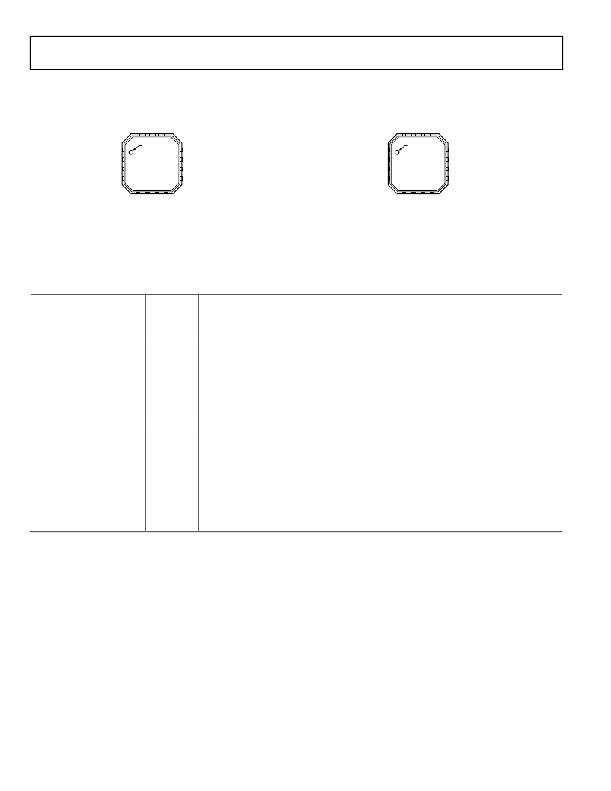
�PIN� CONFIGURATIONS� AND� FUNCTION� DESCRIPTIONS�
�PIN� 1�
�PIN� 1�
�Data� Sheet�
�VIN� 1�
�VIN� 2�
�VIN� 3�
�EN� 4�
�INDICATOR�
�ADP1754�
�TOP� VIEW�
�(Not� to� Scale)�
�12� VOUT�
�11� VOUT�
�10� VOUT�
�9� SENSE�
�VIN� 1�
�VIN� 2�
�VIN� 3�
�EN� 4�
�INDICATOR�
�ADP1755�
�TOP� VIEW�
�(Not� to� Scale)�
�12� VOUT�
�11� VOUT�
�10� VOUT�
�9� ADJ�
�NOTES�
�1.� NC� =� NO� CONNECT.�
�2.� THE� EXPOSED� PAD� ON� THE� BOTTOM� OF� THE� LFCSP� ENHANCES�
�THERMAL� PERFORMANCE� AND� IS� ELECTRICALLY� CONNECTED� TO� GND�
�INSIDE� THE� PACKAGE.� IT� IS� RECOMMENDED� THAT� THE� EXPOSED� PAD�
�BE� CONNECTED� TO� THE� GROUND� PLANE� ON� THE� BOARD.�
�Figure� 3.� ADP1754� Pin� Configuration�
�Table� 5.� Pin� Function� Descriptions�
�NOTES�
�1.� NC� =� NO� CONNECT.�
�2.� THE� EXPOSED� PAD� ON� THE� BOTTOM� OF� THE� LFCSP� ENHANCES�
�THERMAL� PERFORMANCE� AND� IS� ELECTRICALLY� CONNECTED� TO� GND�
�INSIDE� THE� PACKAGE.� IT� IS� RECOMMENDED� THAT� THE� EXPOSED� PAD�
�BE� CONNECTED� TO� THE� GROUND� PLANE� ON� THE� BOARD.�
�Figure� 4.� ADP1755� Pin� Configuration�
�ADP1754�
�ADP1755�
�Pin� No.�
�1,� 2,� 3,� 15,�
�16�
�4�
�Pin� No.�
�1,� 2,� 3,� 15,�
�16�
�4�
�Mnemonic�
�VIN�
�EN�
�Description�
�Regulator� Input� Supply.� Bypass� VIN� to� GND� with� a� 4.7� μF� or� greater� capacitor.� Note� that� all� five�
�VIN� pins� must� be� connected� to� the� source.�
�Enable� Input.� Drive� EN� high� to� turn� on� the� regulator;� drive� it� low� to� turn� off� the� regulator.� For�
�automatic� startup,� connect� EN� to� VIN.�
�5�
�5�
�PG�
�Power� Good.� This� open-drain� output� requires� an� external� pull-up� resistor� to� VIN.� If� the� part� is� in�
�shutdown� mode,� current-limit� mode,� thermal� shutdown,� or� if� it� falls� below� 90%� of� the� nominal�
�output� voltage,� PG� immediately� transitions� low.�
�6�
�7�
�8�
�9�
�6�
�7�
�8�
�N/A�
�GND�
�SS�
�NC�
�SENSE�
�Ground.�
�Soft� Start.� A� capacitor� connected� to� this� pin� determines� the� soft� start� time.�
�Not� Connected.� No� internal� connection.�
�Sense.� This� pin� measures� the� actual� output� voltage� at� the� load� and� feeds� it� to� the� error�
�amplifier.� Connect� SENSE� as� close� as� possible� to� the� load� to� minimize� the� effect� of� IR� drop�
�between� the� regulator� output� and� the� load.�
�N/A�
�10,� 11,� 12,�
�13,� 14�
�17� (EPAD)�
�9�
�10,� 11,� 12,�
�13,� 14�
�17� (EPAD)�
�ADJ�
�VOUT�
�Exposed�
�paddle�
�(EPAD)�
�Adjust.� A� resistor� divider� from� VOUT� to� ADJ� sets� the� output� voltage.�
�Regulated� Output� Voltage.� Bypass� VOUT� to� GND� with� a� 4.7� μF� or� greater� capacitor.� Note� that� all�
�five� VOUT� pins� must� be� connected� to� the� load.�
�The� exposed� pad� on� the� bottom� of� the� LFCSP� package� enhances� thermal� performance� and� is�
�electrically� connected� to� GND� inside� the� package.� It� is� recommended� that� the� exposed� pad� be�
�connected� to� the� ground� plane� on� the� board.�
�Rev.� F� |� Page� 6� of� 20�
�相关PDF资料 |
PDF描述 |
|---|---|
| UZR0G101MCL1GB | CAP ALUM 100UF 4V 20% SMD |
| VE-J5F-CX | CONVERTER MOD DC/DC 72V 75W |
| 63VXG2200MEFCSN25X30 | CAP ALUM 2200UF 63V 20% SNAP-IN |
| EMC31DRYI | CONN EDGECARD 62POS .100 EXTEND |
| 180MXC560MEFCSN22X40 | CAP ALUM 560UF 180V 20% SNAP-IN |
相关代理商/技术参数 |
参数描述 |
|---|---|
| ADP1755-BL1-EVZ | 制造商:Analog Devices 功能描述:Evaluation Board Is Used To Demonstrate The Functionality Of The ADP1752/ADP1753 制造商:Analog Devices 功能描述:BLANK ADISIMPOWER EVAL ADP1755 - Boxed Product (Development Kits) |
| ADP1755-EVALZ | 功能描述:BOARD EVAL 1.2V SET ADP1755 RoHS:是 类别:编程器,开发系统 >> 评估板 - 线性稳压器 (LDO) 系列:- 产品变化通告:1Q2012 Discontinuation 30/Mar/2012 设计资源:NCP590MNDPTAGEVB Gerber Files 标准包装:1 系列:- 每 IC 通道数:2 - 双 输出电压:1.8V,2.8V 电流 - 输出:300mA 输入电压:2.1 ~ 5.5 V 稳压器类型:正,固定式 工作温度:-40°C ~ 85°C 板类型:完全填充 已供物品:板 已用 IC / 零件:NCP590MNDP 其它名称:NCP590MNDPTAGEVB-NDNCP590MNDPTAGEVBOS |
| ADP175ARMZ-0.75R7 | 制造商:AD 制造商全称:Analog Devices 功能描述:500 mA, Low Dropout, CMOS Linear Regulator |
| ADP175ARMZ-0.85R7 | 制造商:AD 制造商全称:Analog Devices 功能描述:500 mA, Low Dropout, CMOS Linear Regulator |
| ADP175ARMZ-0.8-R7 | 制造商:AD 制造商全称:Analog Devices 功能描述:500 mA, Low Dropout, CMOS Linear Regulator |
发布紧急采购,3分钟左右您将得到回复。