- 您现在的位置:买卖IC网 > PDF目录14217 > ADP2105ACPZ-3.3-R7 (Analog Devices Inc)IC REG BUCK SYNC 3.3V 1A 16LFCSP PDF资料下载
参数资料
| 型号: | ADP2105ACPZ-3.3-R7 |
| 厂商: | Analog Devices Inc |
| 文件页数: | 7/36页 |
| 文件大小: | 0K |
| 描述: | IC REG BUCK SYNC 3.3V 1A 16LFCSP |
| 产品培训模块: | Powering 90nm/65nm FPGAs and Processors |
| 设计资源: | Powering the AD9788 Using ADP2105 for Increased Efficiency (CN0141) |
| 标准包装: | 1 |
| 类型: | 降压(降压) |
| 输出类型: | 固定 |
| 输出数: | 1 |
| 输出电压: | 3.3V |
| 输入电压: | 2.7 V ~ 5.5 V |
| PWM 型: | 电流模式 |
| 频率 - 开关: | 1.2MHz |
| 电流 - 输出: | 1A |
| 同步整流器: | 是 |
| 工作温度: | -40°C ~ 125°C |
| 安装类型: | 表面贴装 |
| 封装/外壳: | 16-VQFN 裸露焊盘,CSP |
| 包装: | 标准包装 |
| 供应商设备封装: | 16-LFCSP-VQ |
| 其它名称: | ADP2105ACPZ-3.3-R7DKR |
第1页第2页第3页第4页第5页第6页当前第7页第8页第9页第10页第11页第12页第13页第14页第15页第16页第17页第18页第19页第20页第21页第22页第23页第24页第25页第26页第27页第28页第29页第30页第31页第32页第33页第34页第35页第36页
�� ��
��
��Data� Sheet�
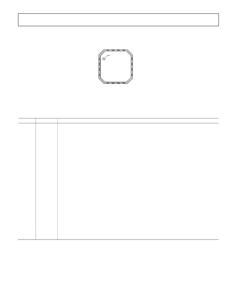
�PIN� CONFIGURATION� AND� FUNCTION� DESCRIPTIONS�
�PIN� 1�
�INDICATOR�
�ADP2105/ADP2106/ADP2107�
�EN� 1�
�12� LX2�
�GND� 2�
�GND� 3�
�ADP2105/�
�ADP2106/�
�ADP2107�
�11� PGND�
�10� LX1�
�GND� 4�
�TOP� VIEW�
�(Not� to� Scale)�
�9�
�PWIN2�
�NOTES�
�1.� NC� =� NO� CONNECT.� DO� NOT� CONNECT� TO� THIS� PIN.�
�2.� THE� EXPOSED� PAD� SHOULD� BE� SOLDERED� TO� AN�
�EXTERNAL� GROUND� PLANE� UNDERNEATH� THE� IC� FOR�
�THERMAL� DISSIPATION.�
�Figure� 4.� Pin� Configuration�
�Table� 4.� Pin� Function� Descriptions�
�Pin� No.�
�1�
�2,� 3,� 4,� 15�
�5�
�6�
�7�
�8�
�9,� 13�
�10,� 12�
�11�
�14�
�16�
�Mnemonic�
�EN�
�GND�
�COMP�
�SS�
�AGND�
�NC�
�PWIN2,�
�PWIN1�
�LX1,� LX2�
�PGND�
�IN�
�FB�
�EP�
�Description�
�Enable� Input.� Drive� EN� high� to� turn� on� the� device.� Drive� EN� low� to� turn� off� the� device� and� reduce� the� input�
�current� to� 0.1� μA.�
�Test� Pins.� These� pins� are� used� for� internal� testing� and� are� not� ground� return� pins.� These� pins� are� to� be� tied� to� the�
�AGND� plane� as� close� as� possible� to� the� ADP2105/ADP2106/ADP2107.�
�Feedback� Loop� Compensation� Node.� COMP� is� the� output� of� the� internal� transconductance� error� amplifier.� Place�
�a� series� RC� network� from� COMP� to� AGND� to� compensate� the� converter.� See� the� Loop� Compensation� section.�
�Soft� Start� Input.� Place� a� capacitor� from� SS� to� AGND� to� set� the� soft� start� period.� A� 1� nF� capacitor� sets� a� 1� ms� soft�
�start� period.�
�Analog� Ground.� Connect� the� ground� of� the� compensation� components,� the� soft� start� capacitor,� and� the� voltage�
�divider� on� the� FB� pin� to� the� AGND� pin� as� close� as� possible� to� the� ADP2105/� ADP2106/ADP2107.� The� AGND� is�
�also� to� be� connected� to� the� exposed� pad� of� ADP2105/ADP2106/ADP2107.�
�No� Connect.� This� is� not� internally� connected� and� can� be� connected� to� other� pins� or� left� unconnected.�
�Power� Source� Inputs.� The� source� of� the� PFET� high-side� switch.� Bypass� each� PWIN� pin� to� the� nearest� PGND� plane� with� a�
�4.7� μF� or� greater� capacitor� as� close� as� possible� to� the� ADP2105/ADP2106/� ADP2107.� See� the� Input� Capacitor�
�Selection� section.�
�Switch� Outputs.� The� drain� of� the� P-channel� power� switch� and� N-channel� synchronous� rectifier.� These� pins� are� to�
�be� tied� together� and� connected� to� the� output� LC� filter� between� LX� and� the� output� voltage.�
�Power� Ground.� Connect� the� ground� return� of� all� input� and� output� capacitors� to� the� PGND� pin� using� a� power�
�ground� plane� as� close� as� possible� to� the� ADP2105/ADP2106/ADP2107.� The� PGND� is� then� to� be� connected� to� the�
�exposed� pad� of� the� ADP2105/ADP2106/ADP2107.�
�Power� Input.� The� power� source� for� the� ADP2105/ADP2106/ADP2107� internal� circuitry.� Connect� IN� and� PWIN1�
�with� a� 10� ?� resistor� as� close� as� possible� to� the� ADP2105/ADP2106/ADP2107.� Bypass� IN� to� AGND� with� a� 0.1� μF� or�
�greater� capacitor.� See� the� Input� Filter� section.�
�Output� Voltage� Sense� or� Feedback� Input.� For� fixed� output� versions,� connect� to� the� output� voltage.� For�
�adjustable� versions,� FB� is� the� input� to� the� error� amplifier.� Drive� FB� through� a� resistive� voltage� divider� to� set� the�
�output� voltage.� The� FB� regulation� voltage� is� 0.8� V.�
�Exposed� Pad.� The� exposed� pad� should� be� soldered� to� an� external� ground� plane� underneath� the� IC� for� thermal�
�dissipation.�
�Rev.� D� |� Page� 7� of� 36�
�相关PDF资料 |
PDF描述 |
|---|---|
| HM66A-03155R6NLF13 | SHIELDED POWER INDUCTORS |
| VI-B7T-EX-F1 | CONVERTER MOD DC/DC 6.5V 75W |
| VI-BW0-EW-F2 | CONVERTER MOD DC/DC 5V 100W |
| EBC28DRES-S93 | CONN EDGECARD 56POS .100 EYELET |
| ADP2105ACPZ-1.5-R7 | IC REG BUCK SYNC 1.5V 1A 16LFCSP |
相关代理商/技术参数 |
参数描述 |
|---|---|
| ADP2105ACPZ-R7 | 功能描述:IC REG BUCK SYNC ADJ 1A 16LFCSP RoHS:是 类别:集成电路 (IC) >> PMIC - 稳压器 - DC DC 开关稳压器 系列:- 标准包装:500 系列:- 类型:切换式电容器(充电泵),反相 输出类型:固定 输出数:1 输出电压:-3V 输入电压:2.3 V ~ 5.5 V PWM 型:Burst Mode? 频率 - 开关:900kHz 电流 - 输出:100mA 同步整流器:无 工作温度:-40°C ~ 85°C 安装类型:表面贴装 封装/外壳:SOT-23-6 细型,TSOT-23-6 包装:带卷 (TR) 供应商设备封装:TSOT-23-6 其它名称:LTC1983ES6-3#TRMTR |
| ADP2105-BL1-EVZ | 功能描述:EVAL BLANK ADISIMPOWER ADP2105 RoHS:是 类别:编程器,开发系统 >> 评估板 - DC/DC 与 AC/DC(离线)SMPS 系列:- 标准包装:1 系列:- 主要目的:DC/DC,步降 输出及类型:1,非隔离 功率 - 输出:- 输出电压:3.3V 电流 - 输出:3A 输入电压:4.5 V ~ 28 V 稳压器拓扑结构:降压 频率 - 开关:250kHz 板类型:完全填充 已供物品:板 已用 IC / 零件:L7981 其它名称:497-12113STEVAL-ISA094V1-ND |
| ADP2105-EVAL | 制造商:Analog Devices 功能描述:EVAL KIT FOR 1 AMP/1.5 AMP/2 AMP SYNCH, STEP-DOWN DC-TO-DC C - Bulk |
| ADP2105-EVALZ | 功能描述:BOARD EVAL 2.5V ADJ ADP2105 RoHS:是 类别:编程器,开发系统 >> 评估板 - DC/DC 与 AC/DC(离线)SMPS 系列:- 产品培训模块:Obsolescence Mitigation Program 标准包装:1 系列:True Shutdown™ 主要目的:DC/DC,步升 输出及类型:1,非隔离 功率 - 输出:- 输出电压:- 电流 - 输出:1A 输入电压:2.5 V ~ 5.5 V 稳压器拓扑结构:升压 频率 - 开关:3MHz 板类型:完全填充 已供物品:板 已用 IC / 零件:MAX8969 |
| ADP2106 | 制造商:AD 制造商全称:Analog Devices 功能描述:1 Amp/1.5 Amp/2 Amp Synchronous, Step-Down DC-to-DC Converters |
发布紧急采购,3分钟左右您将得到回复。