- 您现在的位置:买卖IC网 > PDF目录17413 > ADP2108UJZ-REDYKIT (Analog Devices Inc)KIT REDY TOOL 1.2/3.3 ADP2108 PDF资料下载
参数资料
| 型号: | ADP2108UJZ-REDYKIT |
| 厂商: | Analog Devices Inc |
| 文件页数: | 14/20页 |
| 文件大小: | 0K |
| 描述: | KIT REDY TOOL 1.2/3.3 ADP2108 |
| 标准包装: | 1 |
| 系列: | Redykit™ |
| 主要目的: | DC/DC,步降 |
| 输出及类型: | 1,非隔离 |
| 输出电压: | 1.2V,3.3V |
| 电流 - 输出: | 600mA |
| 输入电压: | 2.3 ~ 5.5 V |
| 稳压器拓扑结构: | 降压 |
| 频率 - 开关: | 3MHz |
| 板类型: | 完全填充 |
| 已供物品: | 2 板,样品 |
| 已用 IC / 零件: | ADP2108 |
�� �
�
�ADP2108�
�12�
�10�
�8�
�6�
�4�
�2�
�Data� Sheet�
�THERMAL� CONSIDERATIONS�
�Because� of� the� high� efficiency� of� the� ADP2108,� only� a� small�
�amount� of� power� is� dissipated� inside� the� ADP2108� package,�
�which� reduces� thermal� constraints.�
�However,� in� applications� with� maximum� loads� at� high� ambient�
�temperature,� low� supply� voltage,� and� high� duty� cycle,� the� heat�
�dissipated� in� the� package� is� great� enough� that� it� may� cause� the�
�junction� temperature� of� the� die� to� exceed� the� maximum�
�junction� temperature� of� 125°C.� If� the� junction� temperature�
�exceeds� 150°C,� the� converter� goes� into� thermal� shutdown.� It�
�recovers� when� the� junction� temperature� falls� below� 130°C.�
�0�
�0�
�1�
�2�
�3�
�4�
�5�
�6�
�The� junction� temperature� of� the� die� is� the� sum� of� the� ambient�
�I� RIPPLE� V� IN�
�(� 2� π� ×� f� SW� )� 2� ×� L� ×� C� OUT�
�ESR� COUT� ≤�
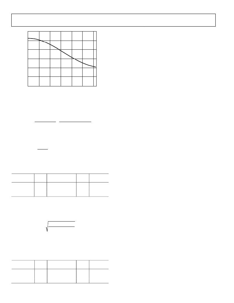
�DC� BIAS� VOLTAGE� (V)�
�Figure� 30.� Typical� Capacitor� Performance�
�The� peak-to-peak� output� voltage� ripple� for� the� selected� output�
�capacitor� and� inductor� values� is� calculated� using� the� following�
�equation:�
�V� RIPPLE� =� ≈�
�8� � f� SW� � C� OUT�
�Capacitors� with� lower� equivalent� series� resistance� (ESR)� are�
�preferred� to� guarantee� low� output� voltage� ripple,� as� shown� in�
�the� following� equation:�
�V� RIPPLE�
�I� RIPPLE�
�The� effective� capacitance� needed� for� stability,� which� includes�
�temperature� and� dc� bias� effects,� is� 7� μF.�
�temperature� of� the� environment� and� the� temperature� rise� of� the�
�package� due� to� power� dissipation,� as� shown� in� the� following�
�equation:�
�T� J� =� T� A� +� T� R�
�where:�
�T� J� is� the� junction� temperature.�
�T� A� is� the� ambient� temperature.�
�T� R� is� the� rise� in� temperature� of� the� package� due� to� power�
�dissipation.�
�The� rise� in� temperature� of� the� package� is� directly� proportional�
�to� the� power� dissipation� in� the� package.� The� proportionality�
�constant� for� this� relationship� is� the� thermal� resistance� from� the�
�junction� of� the� die� to� the� ambient� temperature,� as� shown� in� the�
�following� equation:�
�T� R� =� θ� JA� ×� P� D�
�Table� 7.� Suggested� 10� μF� Capacitors�
�Vendor� Type� Model�
�Case�
�Size�
�Voltage�
�Rating� (V)�
�where:�
�T� R� is� the� rise� in� temperature� of� the� package.�
�θ� JA� is� the� thermal� resistance� from� the� junction� of� the� die� to� the�
�Murata�
�Taiyo� Yuden�
�TDK�
�X5R�
�X5R�
�X5R�
�GRM188R60J106�
�JMK107BJ106�
�C1608JB0J106K�
�0603�
�0603�
�0603�
�6.3�
�6.3�
�6.3�
�ambient� temperature� of� the� package.�
�P� D� is� the� power� dissipation� in� the� package.�
�PCB� LAYOUT� GUIDELINES�
�I� CIN� ≥� I� LOAD� (� MAX� )�
�Input� Capacitor�
�Higher� value� input� capacitors� help� to� reduce� the� input� voltage�
�ripple� and� improve� transient� response.� Maximum� input�
�capacitor� current� is� calculated� using� the� following� equation:�
�V� OUT� (� V� IN� ?� V� OUT� )�
�V� IN�
�Poor� layout� can� affect� ADP2108� performance,� causing� electro-�
�magnetic� interference� (EMI)� and� electromagnetic� compatibility�
�(EMC)� problems,� ground� bounce,� and� voltage� losses.� Poor�
�layout� can� also� affect� regulation� and� stability.� A� good� layout� is�
�implemented� using� the� following� rules:�
�?� Place� the� inductor,� input� capacitor,� and� output� capacitor�
�close� to� the� IC� using� short� tracks.� These� components� carry�
�To� minimize� supply� noise,� place� the� input� capacitor� as� close� to�
�the� VIN� pin� of� the� ADP2108� as� possible.� As� with� the� output�
�capacitor,� a� low� ESR� capacitor� is� recommended.� The� list� of�
��?�
�?�
�high� switching� frequencies,� and� large� tracks� act� as� antennas.�
�Route� the� output� voltage� path� away� from� the� inductor� and�
�SW� node� to� minimize� noise� and� magnetic� interference.�
�Maximize� the� size� of� ground� metal� on� the� component� side�
�Table� 8.� Suggested� 4.7� μF� Capacitors�
�Vendor� Type� Model�
�Murata� X5R� GRM188R60J475�
�Case�
�Size�
�0603�
�Voltage�
�Rating� (V)�
�6.3�
�?�
�to� help� with� thermal� dissipation.�
�Use� a� ground� plane� with� several� vias� connecting� to� the� com-�
�ponent� side� ground� to� further� reduce� noise� interference� on�
�sensitive� circuit� nodes.�
�Taiyo� Yuden�
�TDK�
�X5R�
�X5R�
�JMK107BJ475�
�C1608X5R0J475�
�0603�
�0603�
�6.3�
�6.3�
�Rev.� G� |� Page� 14� of� 20�
�相关PDF资料 |
PDF描述 |
|---|---|
| A9CCA-0306F | FLEX CABLE - AFG03A/AF03/AFG03A |
| RNM-1215S | CONV DC/DC 1W 12VIN 15VOUT |
| MIC5842YV | IC DRVR LATCH 8BIT SER IN 20PLCC |
| A9BBA-0408F | FLEX CABLE - AFF04A/AF04/AFF04A |
| RNM-1209S | CONV DC/DC 1W 12VIN 09VOUT |
相关代理商/技术参数 |
参数描述 |
|---|---|
| ADP2109 | 制造商:AD 制造商全称:Analog Devices 功能描述:Compact 600 mA, 3 MHz, Step-Down Converter with Output Discharge |
| ADP2109ACBZ-1.0-R7 | 功能描述:IC REG BUCK SYNC 1V 0.6A 5WLCSP RoHS:是 类别:集成电路 (IC) >> PMIC - 稳压器 - DC DC 开关稳压器 系列:- 标准包装:500 系列:- 类型:切换式电容器(充电泵),反相 输出类型:固定 输出数:1 输出电压:-3V 输入电压:2.3 V ~ 5.5 V PWM 型:Burst Mode? 频率 - 开关:900kHz 电流 - 输出:100mA 同步整流器:无 工作温度:-40°C ~ 85°C 安装类型:表面贴装 封装/外壳:SOT-23-6 细型,TSOT-23-6 包装:带卷 (TR) 供应商设备封装:TSOT-23-6 其它名称:LTC1983ES6-3#TRMTR |
| ADP2109ACBZ-1.2-R7 | 功能描述:IC REG BUCK SYNC 1.2V .6A 5WLCSP RoHS:是 类别:集成电路 (IC) >> PMIC - 稳压器 - DC DC 开关稳压器 系列:- 标准包装:500 系列:- 类型:切换式电容器(充电泵),反相 输出类型:固定 输出数:1 输出电压:-3V 输入电压:2.3 V ~ 5.5 V PWM 型:Burst Mode? 频率 - 开关:900kHz 电流 - 输出:100mA 同步整流器:无 工作温度:-40°C ~ 85°C 安装类型:表面贴装 封装/外壳:SOT-23-6 细型,TSOT-23-6 包装:带卷 (TR) 供应商设备封装:TSOT-23-6 其它名称:LTC1983ES6-3#TRMTR |
| ADP2109ACBZ-1.5-R7 | 功能描述:IC REG BUCK SYNC 1.5V .6A 5WLCSP RoHS:是 类别:集成电路 (IC) >> PMIC - 稳压器 - DC DC 开关稳压器 系列:- 标准包装:500 系列:- 类型:切换式电容器(充电泵),反相 输出类型:固定 输出数:1 输出电压:-3V 输入电压:2.3 V ~ 5.5 V PWM 型:Burst Mode? 频率 - 开关:900kHz 电流 - 输出:100mA 同步整流器:无 工作温度:-40°C ~ 85°C 安装类型:表面贴装 封装/外壳:SOT-23-6 细型,TSOT-23-6 包装:带卷 (TR) 供应商设备封装:TSOT-23-6 其它名称:LTC1983ES6-3#TRMTR |
| ADP2109ACBZ-1.8-R7 | 功能描述:IC REG BUCK SYNC 1.8V .6A 5WLCSP RoHS:是 类别:集成电路 (IC) >> PMIC - 稳压器 - DC DC 开关稳压器 系列:- 标准包装:500 系列:- 类型:切换式电容器(充电泵),反相 输出类型:固定 输出数:1 输出电压:-3V 输入电压:2.3 V ~ 5.5 V PWM 型:Burst Mode? 频率 - 开关:900kHz 电流 - 输出:100mA 同步整流器:无 工作温度:-40°C ~ 85°C 安装类型:表面贴装 封装/外壳:SOT-23-6 细型,TSOT-23-6 包装:带卷 (TR) 供应商设备封装:TSOT-23-6 其它名称:LTC1983ES6-3#TRMTR |
发布紧急采购,3分钟左右您将得到回复。