- 您现在的位置:买卖IC网 > PDF目录14914 > ADP2127ACNZ1.260R7 (Analog Devices Inc)IC REG BUCK SYNC 1.26V .5A 6EWLP PDF资料下载
参数资料
| 型号: | ADP2127ACNZ1.260R7 |
| 厂商: | Analog Devices Inc |
| 文件页数: | 16/20页 |
| 文件大小: | 0K |
| 描述: | IC REG BUCK SYNC 1.26V .5A 6EWLP |
| 产品变化通告: | 8mm Carrier Tape Changes 28/Feb/2012 |
| 标准包装: | 1 |
| 类型: | 降压(降压) |
| 输出类型: | 固定 |
| 输出数: | 1 |
| 输出电压: | 1.26V |
| 输入电压: | 2.1 V ~ 5.5 V |
| PWM 型: | 电压模式 |
| 频率 - 开关: | 6MHz |
| 电流 - 输出: | 500mA |
| 同步整流器: | 是 |
| 工作温度: | -40°C ~ 85°C |
| 安装类型: | 表面贴装 |
| 封装/外壳: | 6-SMD,无引线 |
| 包装: | 标准包装 |
| 供应商设备封装: | 6-WLP Embedded(1.3x0.90) |
| 其它名称: | ADP2127ACNZ1.260R7DKR |
�� ��
��
��ADP2126/ADP2127�
�Data� Sheet�
�PCB� LAYOUT� GUIDELINES�
�To� ensure� package� reliability,� consider� the� following� guidelines�
�when� designing� the� footprint� for� the� ADP2126/ADP2127.� The�
�BUMPED_CHIP� device� footprint� must� ultimately� be� determined�
�according� to� application� and� customer� specific� reliability�
�requirements,� PCB� fabrication� quality,� and� PCB� assembly�
�capabilities.�
�?�
�?�
�The� Cu� pad� on� the� PCB� for� each� solder� bump� should� be�
�80%� to� 100%� of� the� width� of� the� solder� bump.� A� smaller�
�pad� opening� favors� solder� joint� reliability� (SJR)� performance,�
�whereas� a� larger� pad� opening� favors� drop� test� performance.�
�The� maximum� pad� size,� including� tolerance,� should� not�
�exceed� 180� μm.�
�Electroplated� nickel,� immersion� gold� (ENIG)� and� organic�
�solderability� preservative� (OSP)� were� used� for� internal�
�reliability� testing� and� are� recommended.�
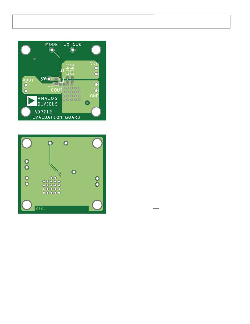
�Figure� 31.� ADP2126� /� ADP2127� Recommended� Top� Layer� Layout�
�Figure� 32.� ADP2126/ADP2127� Recommended� Bottom� Layer� Layout�
�For� high� efficiency,� good� regulation,� and� stability,� a� well-designed�
�and� manufactured� PCB� is� required.�
�Use� the� following� guidelines� when� designing� PCBs:�
�?�
�Keep� the� low� ESR� input� capacitor,� C� IN� ,� close� to� VIN�
�and� GND.�
�?�
�Keep� high� current� traces� as� short� and� as� wide� as� possible.�
�?�
�Avoid� routing� high� impedance� traces� near� any� node�
�connected� to� SW� or� near� the� inductor� to� prevent�
�radiated� noise� injection.�
�?�
�Keep� the� low� ESR� output� capacitor,� C� OUT� ,� close� to� the� FB�
�?�
�?�
�?�
�?�
�?�
�Nonsolder� mask� defined� (NSMD)� Cu� pads� are� recommended�
�for� the� BUMPED_CHIP� package.�
�The� solder� mask� opening� should� be� approximately� 100� μm�
�larger� than� the� pad� opening.�
�The� trace� width� should� be� less� than� two-thirds� the� size� of�
�the� pad� opening.�
�The� routing� of� traces� from� the� Cu� pads� should� be� symmetrical�
�in� X� and� Y� directions.� Symmetrical� routing� of� the� traces�
�prevents� part� rotation� due� to� uneven� solder� wetting/surface�
�tension� forces.�
�Stencil� design� is� important� for� proper� transfer� of� paste� onto�
�the� Cu� pads.� Area� ratio� (AR),� the� relationship� between� the�
�surface� area� of� the� stencil� aperture� and� the� inside� surface�
�area� of� the� aperture� walls,� is� critically� important.� Stencil�
�thickness� has� the� greatest� impact� on� this� ratio.� AR� values�
�from� 0.66� to� 0.8� provide� the� best� paste� transfer� efficiency�
�and� repeatability.� The� AR� is� calculated� from�
�Ap�
�AR� =�
�Aw�
�where:�
�Ap� is� the� area� of� the� aperture� opening.�
�Aw� is� the� wall� area.�
�and� GND� pins� of� the� ADP2126/ADP2127.� Long� trace�
�lengths� from� the� part� to� the� output� capacitor� add� series�
�inductance� that� may� cause� instability� or� increased� ripple.�
�Rev.� B� |� Page� 16� of� 20�
�相关PDF资料 |
PDF描述 |
|---|---|
| GCM36DCMN | CONN EDGECARD 72POS .156 WW |
| PM0805-R15K | INDUCTOR CHIP .15UH 10% SMT |
| H5BXT-10105-W9-ND | JUMPER-H2728TR/C2064W/X 5" |
| H5BXT-10103-N9-ND | JUMPER-H2728TR/C2064N/X 3" |
| ADM8828ARTZ-REEL7 | IC REG SWITCHED CAP INV SOT23-6 |
相关代理商/技术参数 |
参数描述 |
|---|---|
| ADP2138 | 制造商:AD 制造商全称:Analog Devices 功能描述:Compact, 800 mA, 3 MHz, Step-Down DC-to-DC Converter |
| ADP2138ACBZ-0.8-R7 | 功能描述:IC REG BUCK SYNC 0.8V .8A 6WLCSP RoHS:是 类别:集成电路 (IC) >> PMIC - 稳压器 - DC DC 开关稳压器 系列:- 标准包装:500 系列:- 类型:切换式电容器(充电泵),反相 输出类型:固定 输出数:1 输出电压:-3V 输入电压:2.3 V ~ 5.5 V PWM 型:Burst Mode? 频率 - 开关:900kHz 电流 - 输出:100mA 同步整流器:无 工作温度:-40°C ~ 85°C 安装类型:表面贴装 封装/外壳:SOT-23-6 细型,TSOT-23-6 包装:带卷 (TR) 供应商设备封装:TSOT-23-6 其它名称:LTC1983ES6-3#TRMTR |
| ADP2138ACBZ-1.0-R7 | 功能描述:IC REG BUCK SYNC 1V 0.8A 6WLCSP RoHS:是 类别:集成电路 (IC) >> PMIC - 稳压器 - DC DC 开关稳压器 系列:- 标准包装:500 系列:- 类型:切换式电容器(充电泵),反相 输出类型:固定 输出数:1 输出电压:-3V 输入电压:2.3 V ~ 5.5 V PWM 型:Burst Mode? 频率 - 开关:900kHz 电流 - 输出:100mA 同步整流器:无 工作温度:-40°C ~ 85°C 安装类型:表面贴装 封装/外壳:SOT-23-6 细型,TSOT-23-6 包装:带卷 (TR) 供应商设备封装:TSOT-23-6 其它名称:LTC1983ES6-3#TRMTR |
| ADP2138ACBZ-1.2-R7 | 功能描述:IC REG BUCK SYNC 1.2V .8A 6WLCSP RoHS:是 类别:集成电路 (IC) >> PMIC - 稳压器 - DC DC 开关稳压器 系列:- 产品培训模块:High Efficiency Current Mode Switching Regulators CMOS LDO Regulators 特色产品:BD91x Series Step-Down Regulators 标准包装:2,500 系列:- 类型:降压(降压) 输出类型:两者兼有 输出数:2 输出电压:3.3V,0.8 V ~ 2.5 V 输入电压:4.5 V ~ 5.5 V PWM 型:电流模式 频率 - 开关:1MHz 电流 - 输出:1.5A 同步整流器:是 工作温度:-40°C ~ 85°C 安装类型:表面贴装 封装/外壳:20-VFQFN 裸露焊盘 包装:带卷 (TR) 供应商设备封装:VQFN020V4040 产品目录页面:1373 (CN2011-ZH PDF) 其它名称:BD9152MUV-E2TR |
| ADP2138ACBZ-1.5-R7 | 功能描述:IC REG BUCK SYNC 1.5V .8A 6WLCSP RoHS:是 类别:集成电路 (IC) >> PMIC - 稳压器 - DC DC 开关稳压器 系列:- 标准包装:500 系列:- 类型:切换式电容器(充电泵),反相 输出类型:固定 输出数:1 输出电压:-3V 输入电压:2.3 V ~ 5.5 V PWM 型:Burst Mode? 频率 - 开关:900kHz 电流 - 输出:100mA 同步整流器:无 工作温度:-40°C ~ 85°C 安装类型:表面贴装 封装/外壳:SOT-23-6 细型,TSOT-23-6 包装:带卷 (TR) 供应商设备封装:TSOT-23-6 其它名称:LTC1983ES6-3#TRMTR |
发布紧急采购,3分钟左右您将得到回复。