- 您现在的位置:买卖IC网 > PDF目录20700 > ADP2140ACPZ1812R7 (Analog Devices Inc)IC REG DL BCK/LINEAR 10LFCSP PDF资料下载
参数资料
| 型号: | ADP2140ACPZ1812R7 |
| 厂商: | Analog Devices Inc |
| 文件页数: | 28/32页 |
| 文件大小: | 2731K |
| 描述: | IC REG DL BCK/LINEAR 10LFCSP |
| 标准包装: | 1 |
| 拓扑: | 降压(降压)同步(1),线性(LDO)(1) |
| 功能: | 任何功能 |
| 输出数: | 2 |
| 频率 - 开关: | 3MHz |
| 电压/电流 - 输出 1: | 1.8V,600mA |
| 电压/电流 - 输出 2: | 1.2V,300mA |
| 带 LED 驱动器: | 无 |
| 带监控器: | 无 |
| 带序列发生器: | 是 |
| 电源电压: | 1.65 V ~ 5.5 V |
| 工作温度: | -40°C ~ 125°C |
| 安装类型: | 表面贴装 |
| 封装/外壳: | 10-WFDFN 裸露焊盘,CSP |
| 供应商设备封装: | 10-LFCSP-WD(3x3) |
| 包装: | 标准包装 |
| 其它名称: | ADP2140ACPZ1812R7DKR |
第1页第2页第3页第4页第5页第6页第7页第8页第9页第10页第11页第12页第13页第14页第15页第16页第17页第18页第19页第20页第21页第22页第23页第24页第25页第26页第27页当前第28页第29页第30页第31页第32页
ADP2140
Data Sheet
Rev. A | Page 28 of 32
THERMAL CONSIDERATIONS
In most applications, the ADP2140 does not dissipate much
heat due to its high efficiency. However, in applications with
high ambient temperature and high supply voltage-to-output
voltage differential, the heat dissipated in the package is large
enough that it can cause the junction temperature of the die to
exceed the maximum junction temperature of 125癈.
When the junction temperature exceeds 150癈, the converter
enters thermal shutdown. It recovers only after the junction
temperature has decreased below 130癈 to prevent any permanent
damage. Therefore, thermal analysis for the chosen application
is very important to guarantee reliable performance over all
conditions. The junction temperature of the die is the sum of
the ambient temperature of the environment and the tempera-
ture rise of the package due to the power dissipation, as shown
in Equation 2.
To guarantee reliable operation, the junction temperature of the
ADP2140 must not exceed 125癈. To ensure the junction temper-
ature stays below this maximum value, the user needs to be aware
of the parameters that contribute to junction temperature changes.
These parameters include ambient temperature, power dissipa-
tion in the power device, and thermal resistances between the
junction and ambient air (?/DIV>
JA
). The ?/DIV>
JA
number is dependent on
the package assembly compounds that are used and the amount of
copper used to solder the package GND pins to the PCB. Table 10
shows typical ?/DIV>
JA
values of the 10-lead, 3 mm ?3 mm LFCSP for
various PCB copper sizes.
Table 10. Typical ?/DIV>
JA
Values
Copper Size (mm
2
)
?nbsp (癈/W)
0
1
42.5
50
40.0
100
38.8
300
37.2
500
36.2
1
The device is soldered to minimum size pin traces.
The junction temperature of the ADP2140 can be calculated
from the following equation:
T
J
= T
A
+ (P
D
??/DIV>
JA
)
(2)
where:
T
A
is the ambient temperature.
P
D
is the total power dissipation in the die, given by
P
D
= P
LDO
+ P
BUCK
where:
P
LDO
= [(V
IN
V
OUT
) ?I
LOAD
] + (V
IN
?I
AGND
)
(3)
P
BUCK
= P
SW
+ P
TRAN
+ P
SW_COND
(4)
where:
I
LOAD
is the LDO load current.
I
AGND
is the analog ground current.
V
IN
and V
OUT
are the LDO input and output voltages,
respectively.
P
SW
, P
TRAN
, and P
SW_COND
are defined in the Efficiency section.
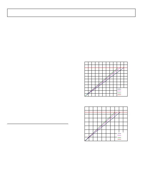
For a given ambient temperature and total power dissipation,
there exists a minimum copper size requirement for the PCB to
ensure the junction temperature does not rise above 125癈. The
following figures show junction temperature calculations for
different ambient temperatures, total power dissipation, and
areas of PCB copper.
145
135
125
115
105
95
85
75
65
55
45
35
25
0 0.25 0.50 0.75 1.00 1.25 1.50 1.75 2.00 2.25 2.50 2.75 3.00
TOTAL POWER DISSIPATION W
500mm
2
50mm
2
0mm
2
T
J MAX
Figure 91. Junction Temperature vs. Power Dissipation, T
A
= 25癈
140
130
120
110
100
90
80
70
60
50
0
0.25 0.50 0.75 1.00 1.25 1.50 1.75 2.00 2.25 2.50
TOTAL POWER DISSIPATION W
500mm
2
50mm
2
0mm
2
T
J MAX
Figure 92. Junction Temperature vs. Power Dissipation, T
A
= 50癈
相关PDF资料 |
PDF描述 |
|---|---|
| GCC22DCAN | CONN EDGECARD 44POS R/A .100 SLD |
| ADP2140ACPZ1833R7 | IC REG DL BCK/LINEAR 10LFCSP |
| LM2795TL | IC LED DRVR WHT BCKLT 14MICROSMD |
| LM2795BLX/NOPB | IC LED DRVR WHT BCKLT 14MICROSMD |
| GCC22DCAH | CONN EDGECARD 44POS R/A .100 SLD |
相关代理商/技术参数 |
参数描述 |
|---|---|
| ADP2140ACPZ1815R7 | 功能描述:IC REG DL BCK/LINEAR 10LFCSP RoHS:是 类别:集成电路 (IC) >> PMIC - 稳压器 - 线性 + 切换式 系列:- 标准包装:2,500 系列:- 拓扑:降压(降压)同步(3),线性(LDO)(2) 功能:任何功能 输出数:5 频率 - 开关:300kHz 电压/电流 - 输出 1:控制器 电压/电流 - 输出 2:控制器 电压/电流 - 输出 3:控制器 带 LED 驱动器:无 带监控器:无 带序列发生器:是 电源电压:5.6 V ~ 24 V 工作温度:-40°C ~ 85°C 安装类型:* 封装/外壳:* 供应商设备封装:* 包装:* |
| ADP2140ACPZ1833R7 | 功能描述:IC REG DL BCK/LINEAR 10LFCSP RoHS:是 类别:集成电路 (IC) >> PMIC - 稳压器 - 线性 + 切换式 系列:- 标准包装:2,500 系列:- 拓扑:降压(降压)同步(3),线性(LDO)(2) 功能:任何功能 输出数:5 频率 - 开关:300kHz 电压/电流 - 输出 1:控制器 电压/电流 - 输出 2:控制器 电压/电流 - 输出 3:控制器 带 LED 驱动器:无 带监控器:无 带序列发生器:是 电源电压:5.6 V ~ 24 V 工作温度:-40°C ~ 85°C 安装类型:* 封装/外壳:* 供应商设备封装:* 包装:* |
| ADP2140ACPZ18812R7 | 功能描述:IC REG DL BCK/LINEAR 10LFCSP RoHS:是 类别:集成电路 (IC) >> PMIC - 稳压器 - 线性 + 切换式 系列:- 标准包装:2,500 系列:- 拓扑:降压(降压)同步(3),线性(LDO)(2) 功能:任何功能 输出数:5 频率 - 开关:300kHz 电压/电流 - 输出 1:控制器 电压/电流 - 输出 2:控制器 电压/电流 - 输出 3:控制器 带 LED 驱动器:无 带监控器:无 带序列发生器:是 电源电压:5.6 V ~ 24 V 工作温度:-40°C ~ 85°C 安装类型:* 封装/外壳:* 供应商设备封装:* 包装:* |
| ADP2140ACPZ2518R7 | 功能描述:IC REG DL BCK/LINEAR 10LFCSP RoHS:是 类别:集成电路 (IC) >> PMIC - 稳压器 - 线性 + 切换式 系列:- 标准包装:2,500 系列:- 拓扑:降压(降压)同步(3),线性(LDO)(2) 功能:任何功能 输出数:5 频率 - 开关:300kHz 电压/电流 - 输出 1:控制器 电压/电流 - 输出 2:控制器 电压/电流 - 输出 3:控制器 带 LED 驱动器:无 带监控器:无 带序列发生器:是 电源电压:5.6 V ~ 24 V 工作温度:-40°C ~ 85°C 安装类型:* 封装/外壳:* 供应商设备封装:* 包装:* |
| ADP2140ACPZ3312R7 | 功能描述:IC REG DL BCK/LINEAR 10LFCSP RoHS:是 类别:集成电路 (IC) >> PMIC - 稳压器 - 线性 + 切换式 系列:- 标准包装:2,500 系列:- 拓扑:降压(降压)同步(3),线性(LDO)(2) 功能:任何功能 输出数:5 频率 - 开关:300kHz 电压/电流 - 输出 1:控制器 电压/电流 - 输出 2:控制器 电压/电流 - 输出 3:控制器 带 LED 驱动器:无 带监控器:无 带序列发生器:是 电源电压:5.6 V ~ 24 V 工作温度:-40°C ~ 85°C 安装类型:* 封装/外壳:* 供应商设备封装:* 包装:* |
发布紧急采购,3分钟左右您将得到回复。