- 您现在的位置:买卖IC网 > PDF目录20698 > ADP2140ACPZ3318R7 (Analog Devices Inc)IC REG DL BCK/LINEAR 10LFCSP PDF资料下载
参数资料
| 型号: | ADP2140ACPZ3318R7 |
| 厂商: | Analog Devices Inc |
| 文件页数: | 24/32页 |
| 文件大小: | 2731K |
| 描述: | IC REG DL BCK/LINEAR 10LFCSP |
| 标准包装: | 1 |
| 拓扑: | 降压(降压)同步(1),线性(LDO)(1) |
| 功能: | 任何功能 |
| 输出数: | 2 |
| 频率 - 开关: | 3MHz |
| 电压/电流 - 输出 1: | 3.3V,600mA |
| 电压/电流 - 输出 2: | 1.8V,300mA |
| 带 LED 驱动器: | 无 |
| 带监控器: | 无 |
| 带序列发生器: | 是 |
| 电源电压: | 1.65 V ~ 5.5 V |
| 工作温度: | -40°C ~ 125°C |
| 安装类型: | 表面贴装 |
| 封装/外壳: | 10-WFDFN 裸露焊盘,CSP |
| 供应商设备封装: | 10-LFCSP-WD(3x3) |
| 包装: | 标准包装 |
| 其它名称: | ADP2140ACPZ3318R7DKR |
第1页第2页第3页第4页第5页第6页第7页第8页第9页第10页第11页第12页第13页第14页第15页第16页第17页第18页第19页第20页第21页第22页第23页当前第24页第25页第26页第27页第28页第29页第30页第31页第32页
ADP2140
Data Sheet
Rev. A | Page 24 of 32
CH1 500mV
CH2 500mV
M40.0祍
A CH3 1.16V
T 10.00%
CH3 2.00V
T
LDO OUTPUT
BUCK OUTPUT
EN1
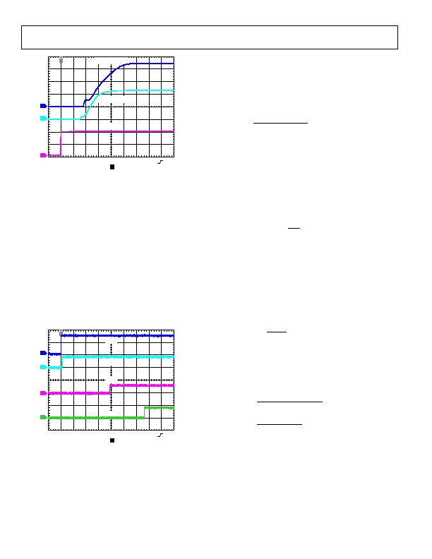
Figure 84. Individual Activation Mode, EN1 and EN2 Pins Tied Together
POWER-GOOD FUNCTION
The ADP2140 power-good (PG) pin indicates the state of the
monitored output voltages. The PG function is the logical AND
of the state of both outputs. The PG function is an active high,
open-drain output, requiring an external pull-up resistor typically
supplied from the I/O supply rail, as shown in . When the sensed
output voltages are below 92% of their nominal value, the PG pin is
held low. When the sensed output voltages rise above 92% of
the nominal levels, the PG line is pulled high after t
RESET
. The
PG pin remains high as long as the sensed output voltages are
above 86% of the nominal output voltage levels.
The typical PG delay when the buck is in PWM mode is 5 ms.
When the part is in PSM mode, the PG delay is load dependent
because the internal clock is disabled to reduce quiescent current
during the sleep stage. PG delay varies from hundreds of micro-
seconds at 10 mA, up to seconds at current loads of less than 10 糀.
CH1 2.00V
CH2 2.00V
CH4 2.00V
M2.00ms
A CH1 2.20V
T 10.20%
CH3 2.00V
T
EN1
BUCK
LDO
PG
Figure 85. Typical PG Timing
EXTERNAL COMPONENT SELECTION
The external component selection for the ADP2140 application
circuit that is shown in Table 8, Table 9, and Figure 86 is dependent
on input voltage, output voltage, and load current requirements.
Additionally, trade-offs between performance parameters such
as efficiency and transient response can be made by varying the
choice of external components.
SELECTING THE INDUCTOR
The high frequency switching of the ADP2140 allows the selection
of small chip inductors. The inductor value affects the transi-
tion between CFM to PSM, efficiency, output ripple, and current
limit values. Use the following equation to calculate the inductor
ripple current:
L
f
V
V
V
V
I
sw
IN
OUT
IN
OUT
L
?/DIV>
?/DIV>
?/DIV>
=
)
(
where:
f
SW
is the switching frequency (3 MHz typical).
L is the inductor value.
The dc resistance (DCR) value of the selected inductor affects
efficiency, but a decrease in this value typically means an increase
in root mean square (rms) losses in the core and skin. As a
minimum requirement, the dc current rating of the inductor
should be equal to the maximum load current plus half of the
inductor current ripple, as shown by the following equation:
)
2
?/DIV>
(
)
(
L
MAX
LOAD
PK
I
I
+
=
OUTPUT CAPACITOR
Output capacitance is required to minimize the voltage over-
shoot and ripple present on the output. Capacitors with low
equivalent series resistance (ESR) values produce the lowest
output ripple; therefore, use capacitors such as the X5R dielectric.
Do not use the Y5V and Z5U capacitors; they are not suitable
for this application because of their large variation in capacitance
over temperature and dc bias voltage. Because ESR is important,
select the capacitor using the following equation:
L
RIPPLE
COUT
I
V
SR
?/DIV>
d
where:
ESR
COUT
is the ESR of the chosen capacitor.
V
RIPPLE
is the peak-to-peak output voltage ripple.
Use the following equations to determine the output
capacitance:
RIPPLE
SW
IN
OUT
V
L
f
?/DIV>
V
?/DIV>
?/DIV>
?/DIV>
e
2
)
2
(
OUT
SW
L
OUT
V
f
I
?/DIV>
8
?/DIV>
?/DIV>
?/DIV>
e
Increasing the output capacitor has no effect on stability and
increasing the output capacitance may further reduce output
ripple and enhance load transient response. When choosing this
value, it is also important to account for the loss of capacitance
due to output voltage dc bias.
INPUT CAPACITOR
Input capacitance is required to reduce input voltage ripple; there-
fore, place the input capacitor as close as possible to the VINx
pins. As with the output capacitor, a low ESR X7R- or X5R-type
相关PDF资料 |
PDF描述 |
|---|---|
| SE07PJ-E3/85A | DIODE ESD 0.7A 600V DO-220AA |
| GEC19DREF | CONN EDGECARD 38POS .100 EYELET |
| SE07PG-E3/85A | DIODE ESD 0.7A 400V DO-220AA |
| HSM43DRTI | CONN EDGECARD 86POS DIP .156 SLD |
| SE07PD-E3/85A | DIODE ESD 0.7A 200V DO-220AA |
相关代理商/技术参数 |
参数描述 |
|---|---|
| ADP2140ACPZ3325R7 | 功能描述:IC REG DL BCK/LINEAR 10LFCSP RoHS:是 类别:集成电路 (IC) >> PMIC - 稳压器 - 线性 + 切换式 系列:- 标准包装:2,500 系列:- 拓扑:降压(降压)同步(3),线性(LDO)(2) 功能:任何功能 输出数:5 频率 - 开关:300kHz 电压/电流 - 输出 1:控制器 电压/电流 - 输出 2:控制器 电压/电流 - 输出 3:控制器 带 LED 驱动器:无 带监控器:无 带序列发生器:是 电源电压:5.6 V ~ 24 V 工作温度:-40°C ~ 85°C 安装类型:* 封装/外壳:* 供应商设备封装:* 包装:* |
| ADP2140ACPZ3328R7 | 功能描述:IC REG DL BCK/LINEAR 10LFCSP RoHS:是 类别:集成电路 (IC) >> PMIC - 稳压器 - 线性 + 切换式 系列:- 标准包装:2,500 系列:- 拓扑:降压(降压)同步(3),线性(LDO)(2) 功能:任何功能 输出数:5 频率 - 开关:300kHz 电压/电流 - 输出 1:控制器 电压/电流 - 输出 2:控制器 电压/电流 - 输出 3:控制器 带 LED 驱动器:无 带监控器:无 带序列发生器:是 电源电压:5.6 V ~ 24 V 工作温度:-40°C ~ 85°C 安装类型:* 封装/外壳:* 供应商设备封装:* 包装:* |
| ADP2140CPZ-REDYKIT | 功能描述:REDYKIT 2 BOARDS ADP2140ACPZ RoHS:是 类别:编程器,开发系统 >> 评估板 - 线性稳压器 (LDO) 系列:* 产品变化通告:1Q2012 Discontinuation 30/Mar/2012 设计资源:NCP590MNDPTAGEVB Gerber Files 标准包装:1 系列:- 每 IC 通道数:2 - 双 输出电压:1.8V,2.8V 电流 - 输出:300mA 输入电压:2.1 ~ 5.5 V 稳压器类型:正,固定式 工作温度:-40°C ~ 85°C 板类型:完全填充 已供物品:板 已用 IC / 零件:NCP590MNDP 其它名称:NCP590MNDPTAGEVB-NDNCP590MNDPTAGEVBOS |
| ADP2147 | 制造商:AD 制造商全称:Analog Devices 功能描述:Compact, 800 mA, 3 MHz, Simple DVS, Buck Regulator Input voltage: 2.3 V to 5.5 V |
| ADP2147ACBZ-110-R7 | 功能描述:IC REG BUCK SYNC 0.8A 6WLCSP RoHS:是 类别:集成电路 (IC) >> PMIC - 稳压器 - DC DC 开关稳压器 系列:- 产品培训模块:High Efficiency Current Mode Switching Regulators CMOS LDO Regulators 特色产品:BD91x Series Step-Down Regulators 标准包装:2,500 系列:- 类型:降压(降压) 输出类型:两者兼有 输出数:2 输出电压:3.3V,0.8 V ~ 2.5 V 输入电压:4.5 V ~ 5.5 V PWM 型:电流模式 频率 - 开关:1MHz 电流 - 输出:1.5A 同步整流器:是 工作温度:-40°C ~ 85°C 安装类型:表面贴装 封装/外壳:20-VFQFN 裸露焊盘 包装:带卷 (TR) 供应商设备封装:VQFN020V4040 产品目录页面:1373 (CN2011-ZH PDF) 其它名称:BD9152MUV-E2TR |
发布紧急采购,3分钟左右您将得到回复。