参数资料
| 型号: | ADP220ACBZ-2828R7 |
| 厂商: | Analog Devices Inc |
| 文件页数: | 11/20页 |
| 文件大小: | 0K |
| 描述: | IC REG LDO 2.8V .2A 6WLCSP |
| 产品变化通告: | 8mm Carrier Tape Changes 28/Feb/2012 |
| 标准包装: | 1 |
| 稳压器拓扑结构: | 正,固定式 |
| 输出电压: | 2.8V |
| 输入电压: | 2.5 V ~ 5.5 V |
| 电压 - 压降(标准): | 0.15V @ 200mA |
| 稳压器数量: | 2 |
| 电流 - 输出: | 200mA(最小值) |
| 电流 - 限制(最小): | 240mA |
| 工作温度: | -40°C ~ 125°C |
| 安装类型: | 表面贴装 |
| 封装/外壳: | 6-WFBGA,WLCSP |
| 供应商设备封装: | 6-WLCSP(1.45x0.95) |
| 包装: | 标准包装 |
| 其它名称: | ADP220ACBZ-2828R7DKR |
�� ��
��
��Data� Sheet�
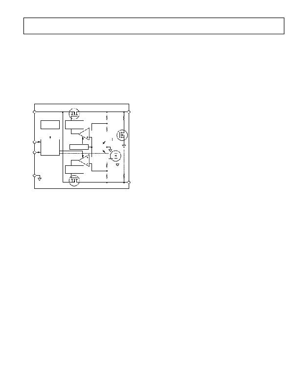
�THEORY� OF� OPERATION�
�The� ADP220/ADP221� are� low� quiescent� current,� low� dropout�
�linear� regulators� that� operate� from� 2.5� V� to� 5.5� V� and� provide�
�up� to� 200� mA� of� current� from� each� output.� Drawing� a� low� 120� μA�
�quiescent� current� (typical)� at� full� load� makes� the� ADP220/�
�ADP221� ideal� for� battery-operated� portable� equipment.� Shut-�
�down� current� consumption� is� typically� 100� nA.�
�Optimized� for� use� with� small� 1� μF� ceramic� capacitors,� the�
�ADP220/ADP221� provide� excellent� transient� performance.�
�ADP220/ADP221�
�Internally,� the� ADP220/ADP221� consist� of� a� reference,� two� error�
�amplifiers,� two� feedback� voltage� dividers,� and� two� PMOS� pass�
�transistors.� Output� current� is� delivered� via� the� PMOS� pass� device,�
�which� is� controlled� by� the� error� amplifier.� The� error� amplifier�
�compares� the� reference� voltage� with� the� feedback� voltage� from�
�the� output� and� amplifies� the� difference.� If� the� feedback� voltage�
�is� lower� than� the� reference� voltage,� the� gate� of� the� PMOS� device�
�is� pulled� lower,� allowing� more� current� to� flow� and� increasing�
�the� output� voltage.� If� the� feedback� voltage� is� higher� than� the�
�reference� voltage,� the� gate� of� the� PMOS� device� is� pulled� higher,�
�VIN�
�THERMAL�
�SHUTDOWN�
�CURRENT�
�LIMIT�
�60Ω�
�VOUT1�
�allowing� less� current� to� flow� and� decreasing� the� output� voltage.�
�The� ADP221� also� includes� an� active� pull-down� circuit� to� rapidly�
�discharge� the� output� load� capacitance� when� each� output� is�
�disabled.�
�EN1�
�EN2�
�CONTROL�
�LOGIC�
�AND�
�ENABLE�
�REFERENCE�
�ADP221�
�ONLY�
�The� ADP220/ADP221� are� available� in� multiple� output� voltage�
�options� ranging� from� 0.8� V� to� 3.3� V.� The� ADP220/ADP221� use�
�the� EN1/EN2� pins� to� enable� and� disable� the� VOUT1/VOUT2�
�pins� under� normal� operating� conditions.� When� EN1/EN2� are� high,�
�VOUT1/VOUT2� turn� on;� when� EN1/EN2� are� low,� VOUT1/�
�GND�
�ADP220�
�CURRENT�
�LIMIT�
�60Ω�
�VOUT2� turn� off.� For� automatic� startup,� EN1/EN2� can� be� tied�
�to� VIN.�
�VOUT2�
�Figure� 28.� Internal� Block� Diagram�
�Rev.� H� |� Page� 11� of� 20�
�相关PDF资料 |
PDF描述 |
|---|---|
| ESM22DWWI | CONN EDGECARD 44POS .156 SQ WW |
| GCB85DHLN | CONN EDGECARD 170PS .050 DIP SLD |
| ADP322ACPZ-189-R7 | IC REG LDO 2.5/1.8/1.2V 16LFCSP |
| ADP322ACPZ-145-R7 | IC REG LDO 3.3/2.5/1.2V 16LFCSP |
| MIC5305-4.75YD5 TR | IC REG LDO 4.75V .15A TSOT23-5 |
相关代理商/技术参数 |
参数描述 |
|---|---|
| ADP220ACBZ-3033R7 | 功能描述:Linear Voltage Regulator IC Positive Fixed 2 Output 3V, 3.3V 200mA 6-WLCSP (1.45x0.95) 制造商:analog devices inc. 系列:- 包装:带卷(TR) 零件状态:上次购买时间 稳压器拓扑:正,固定式 电压 - 输出:3V,3.3V 电流 - 输出:200mA 电压 - 跌落(典型值):-,0.15V @ 200mA 稳压器数:2 电压 - 输入:2.5 V ~ 5.5 V 电流 - 限制(最小值):240mA 工作温度:-40°C ~ 125°C 安装类型:表面贴装 封装/外壳:6-WFBGA,WLCSP 供应商器件封装:6-WLCSP(1.45x0.95) 标准包装:1 |
| ADP221ACBZ-1818-R7 | 功能描述:线性稳压器 - 标准 High PSRR Low Noise DUAL Ldo RoHS:否 制造商:STMicroelectronics 输出类型: 极性: 输出电压:1.8 V 输出电流:150 mA 负载调节: 最大输入电压:5.5 V 线路调整率: 最大工作温度:+ 125 C 安装风格:SMD/SMT 封装 / 箱体:SOT-323-5L |
| ADP221ACBZ2828-R7 | 功能描述:线性稳压器 - 标准 High PSRR Low Noise DUAL Ldo RoHS:否 制造商:STMicroelectronics 输出类型: 极性: 输出电压:1.8 V 输出电流:150 mA 负载调节: 最大输入电压:5.5 V 线路调整率: 最大工作温度:+ 125 C 安装风格:SMD/SMT 封装 / 箱体:SOT-323-5L |
| ADP221ACDZ-1818-R7 | 功能描述:线性稳压器 - 标准 RoHS:否 制造商:STMicroelectronics 输出类型: 极性: 输出电压:1.8 V 输出电流:150 mA 负载调节: 最大输入电压:5.5 V 线路调整率: 最大工作温度:+ 125 C 安装风格:SMD/SMT 封装 / 箱体:SOT-323-5L |
| ADP222 | 制造商:AD 制造商全称:Analog Devices 功能描述:Dual, 300 mA Output, Low Noise |
发布紧急采购,3分钟左右您将得到回复。