- 您现在的位置:买卖IC网 > PDF目录17399 > ADP2303-EVALZ (Analog Devices Inc)EVAL BOARD FOR ADP2303 PDF资料下载
参数资料
| 型号: | ADP2303-EVALZ |
| 厂商: | Analog Devices Inc |
| 文件页数: | 17/28页 |
| 文件大小: | 0K |
| 描述: | EVAL BOARD FOR ADP2303 |
| 标准包装: | 1 |
| 主要目的: | DC/DC,步降 |
| 输出及类型: | 1,非隔离 |
| 电流 - 输出: | 3A |
| 输入电压: | 3 ~ 20 V |
| 稳压器拓扑结构: | 降压 |
| 频率 - 开关: | 700kHz |
| 板类型: | 完全填充 |
| 已供物品: | 板 |
| 已用 IC / 零件: | ADP2303 |
第1页第2页第3页第4页第5页第6页第7页第8页第9页第10页第11页第12页第13页第14页第15页第16页当前第17页第18页第19页第20页第21页第22页第23页第24页第25页第26页第27页第28页
�� �
�
�Data� Sheet�
�ADP2302/ADP2303�
�22�
�20�
�V� IN�
�VIN�
�18�
�16�
�M� AXIMUM INPUT VOLTAG� E�
�R� EN1�
�ADP2302/�
�ADP2303�
�14�
�12�
�10�
�R� EN2�
�EN�
�8�
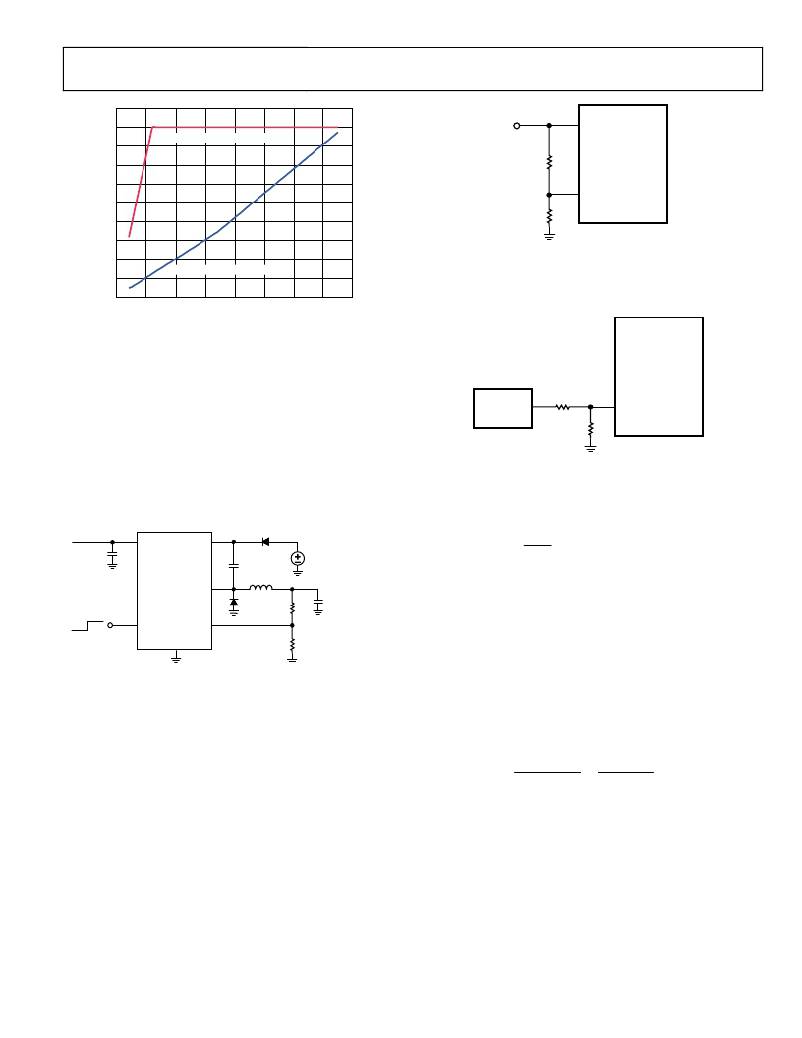
�Figure� 49.� Precision� Enable� Used� as� a� Programmable� UVLO�
�6�
�4�
�2�
�0�
�2�
�M� INIMUM INPUT VOLTAGE�
�4� 6� 8� 10�
�12�
�14�
�16�
�The� precision� enable� feature� also� allows� the� ADP2302/ADP2303� to�
�be� sequenced� precisely� by� using� a� resistive� voltage� divider� from�
��V� OUT� (V)�
�Figure� 47.� Voltage� Conversion� Limitations�
�LOW� INPUT� VOLTAGE� CONSIDERATIONS�
�For� low� input� voltage� between� 3� V� and� 5� V,� the� internal� boot�
�ADP2302/�
�ADP2303�
�regulator� cannot� provide� enough� bootstrap� voltage� due� to� the�
�internal� dropout� voltage.� As� a� result,� the� increased� MOSFET�
�R� DS(ON)� reduces� the� available� load� current.� To� prevent� this,� add�
�ANOTHER�
�DC/DC�
�SUPPLIER�
�R� EN1�
�R� EN2�
�EN�
�an� external� small-signal� Schottky� diode� from� a� 5.0� V� external�
�V� STARTUP� ?� ?� ?�
�?� 1� .� 2� μA� ?� ?� ?� R� EN1� ?� 1� .� 2� V�
�bootstrap� bias� voltage.� Because� the� absolute� maximum� rating�
�between� the� BST� and� SW� pins� is� 6.0� V,� the� bias� voltage� should�
�be� less� than� 5.5� V.� Figure� 48� shows� the� application� diagram� for�
�the� external� bootstrap� circuit.�
�SCHOTTKY�
�3.0V� ~� 5.0V� DIODE�
�VIN� BST�
�ADP2302/� 5V� BIAS� VOLTAGE�
�ADP2303�
�SW�
�Figure� 50.� Precision� Enable� Used� as� a� Sequencing� Control�
�from� Another� DC-to-DC� Power� Supply�
�With� a� 1.2� μA� pull-down� current� on� the� EN� pin,� the� equation� for�
�the� start-up� voltage� in� Figure� 49� and� Figure� 50� is�
�?� 1 . 2 V� ?�
�?� R� EN2� ?�
�where:�
�V� STARTUP� is� the� start-up� voltage� to� enable� the� chip.�
�OFF�
�ON�
�EN�
�FB�
�R� EN1� is� the� resistor� from� the� dc� source� to� EN.�
�R� EN2� is� the� resistor� from� EN� to� GND.�
�?� ?� ?�
�(� V� IN� ?� V� OUT� )� ?� V� OUT� ?� V� D� ?�
�?� I� RIPPLE� ?�
�?�
�GND�
�Figure� 48.� External� Bootstrap� Circuit� for� Low� Input� Voltage� Application�
�PROGRAMMING� THE� PRECISION� ENABLE�
�Generally,� the� EN� pin� can� connect� to� the� VIN� pin� so� that� the�
�device� automatically� starts� up� when� the� input� power� is� applied.�
�However,� the� precision� enabling� feature� allows� the� ADP2302/�
�ADP2303� to� be� used� as� a� programmable� UVLO� by� connecting�
�a� resistive� voltage� divider� to� VIN,� as� shown� in� Figure� 49.� This�
�configuration� prevents� the� start-up� problems� that� can� occur�
�when� VIN� ramps� up� slowly� in� soft� start� with� a� relatively� high�
�load� current.�
�INDUCTOR�
�The� high� switching� frequency� of� the� ADP2302/ADP2303� allows�
�the� use� of� small� inductors.� For� best� performance,� use� inductor�
�values� between� 1� μH� and� 15� μH.�
�The� peak-to-peak� inductor� ripple� current� is� calculated� using� the�
�following� equation:�
�?�
�L� ?� f� sw� ?� V� IN� ?� V� D� ?�
�where:�
�f� SW� is� the� switching� frequency.�
�L� is� the� inductor� value.�
�V� D� is� the� diode� forward� drop.�
�V� IN� is� the� input� voltage.�
�V� OUT� is� the� output� voltage.�
�Inductors� of� smaller� values� are� usually� smaller� in� size� but�
�increase� the� ripple� current� and� the� output� ripple� voltage.� As� a�
�guideline,� the� inductor� peak-to-peak� ripple� current� is� typically�
�set� to� 30%� of� the� maximum� load� current� for� optimal� transient�
�Rev.� A� |� Page� 17� of� 28�
�相关PDF资料 |
PDF描述 |
|---|---|
| RB-3.324D | CONV DC/DC 1W 3.3VIN +/-24VOUT |
| ECE-V0JA220SR | CAP ALUM 22UF 6.3V 20% SMD |
| HCC10DRTN-S13 | CONN EDGECARD 20POS .100 EXTEND |
| RB-3.315D | CONV DC/DC 1W 3.3VIN +/-15VOUT |
| TH3D336M020C0600 | CAP TANT 33UF 20V 20% 2917 |
相关代理商/技术参数 |
参数描述 |
|---|---|
| ADP2303-EVALZ | 制造商:Analog Devices 功能描述:ADP2303, DC TO DC REGULATOR, STEP DOWN, |
| ADP2311-1-EVALZ | 功能描述:ADP2311 - DC/DC, Step Down 2, Non-Isolated Outputs Evaluation Board 制造商:analog devices inc. 系列:- 零件状态:有效 主要用途:DC/DC,步降 输出和类型:2,非隔离 功率 - 输出:- 电压 - 输出:1.2V,3.3V 电流 - 输出:1A,1A 电压 - 输入:4.5 V ~ 18 V 稳压器拓扑:降压 频率 - 开关:300kHz 板类型:完全填充 所含物品:板 使用的 IC/零件:ADP2311 标准包装:1 |
| ADP2311ACPZ-1-R7 | 功能描述:Buck Switching Regulator IC Positive Adjustable 0.6V 2 Output 1A 24-WFQFN Exposed Pad, CSP 制造商:analog devices inc. 系列:- 包装:剪切带(CT) 零件状态:有效 功能:降压 输出配置:正 拓扑:降压 输出类型:可调式 输出数:2 电压 - 输入(最小值):4.5V 电压 - 输入(最大值):18V 电压 - 输出(最小值/固定):0.6V 电压 - 输出(最大值):18V 电流 - 输出:1A 频率 - 开关:300kHz 同步整流器:是 工作温度:-40°C ~ 125°C (TJ) 安装类型:表面贴装 封装/外壳:24-WFQFN 裸露焊盘,CSP 供应商器件封装:24-LFCSP-WQ(4x4) 标准包装:1 |
| ADP2311ACPZ-2-R7 | 功能描述:Buck Switching Regulator IC Positive Adjustable 0.6V 2 Output 1A 24-WFQFN Exposed Pad, CSP 制造商:analog devices inc. 系列:- 包装:剪切带(CT) 零件状态:有效 功能:降压 输出配置:正 拓扑:降压 输出类型:可调式 输出数:2 电压 - 输入(最小值):4.5V 电压 - 输入(最大值):18V 电压 - 输出(最小值/固定):0.6V 电压 - 输出(最大值):18V 电流 - 输出:1A 频率 - 开关:300kHz 同步整流器:是 工作温度:-40°C ~ 125°C (TJ) 安装类型:表面贴装 封装/外壳:24-WFQFN 裸露焊盘,CSP 供应商器件封装:24-LFCSP-WQ(4x4) 标准包装:1 |
| ADP2311ACPZ-3-R7 | 功能描述:Buck Switching Regulator IC Positive Adjustable 0.6V 2 Output 1A 24-WFQFN Exposed Pad, CSP 制造商:analog devices inc. 系列:- 包装:剪切带(CT) 零件状态:有效 功能:降压 输出配置:正 拓扑:降压 输出类型:可调式 输出数:2 电压 - 输入(最小值):4.5V 电压 - 输入(最大值):18V 电压 - 输出(最小值/固定):0.6V 电压 - 输出(最大值):18V 电流 - 输出:1A 频率 - 开关:300kHz 同步整流器:是 工作温度:-40°C ~ 125°C (TJ) 安装类型:表面贴装 封装/外壳:24-WFQFN 裸露焊盘,CSP 供应商器件封装:24-LFCSP-WQ(4x4) 标准包装:1 |
发布紧急采购,3分钟左右您将得到回复。