- 您现在的位置:买卖IC网 > PDF目录14896 > ADP2303ARDZ-5.0-R7 (Analog Devices Inc)IC REG BUCK 5V 3A 8SOIC PDF资料下载
参数资料
| 型号: | ADP2303ARDZ-5.0-R7 |
| 厂商: | Analog Devices Inc |
| 文件页数: | 16/28页 |
| 文件大小: | 0K |
| 描述: | IC REG BUCK 5V 3A 8SOIC |
| 标准包装: | 1 |
| 类型: | 降压(降压) |
| 输出类型: | 固定 |
| 输出数: | 1 |
| 输出电压: | 5V |
| 输入电压: | 3 V ~ 20 V |
| PWM 型: | 电流模式 |
| 频率 - 开关: | 700kHz |
| 电流 - 输出: | 3A |
| 同步整流器: | 无 |
| 工作温度: | -40°C ~ 125°C |
| 安装类型: | 表面贴装 |
| 封装/外壳: | 8-SOIC(0.154",3.90mm Width)裸露焊盘 |
| 包装: | 标准包装 |
| 供应商设备封装: | 8-SOIC-EP |
| 其它名称: | ADP2303ARDZ-5.0-R7DKR |
第1页第2页第3页第4页第5页第6页第7页第8页第9页第10页第11页第12页第13页第14页第15页当前第16页第17页第18页第19页第20页第21页第22页第23页第24页第25页第26页第27页第28页
�� ��
��
��?�
�V� OUT� ?� 0� .� 800� V� ?� ?� ?� 1� ?� TOP�
�?�
�ADP2302/ADP2303�
�APPLICATIONS� INFORMATION�
�ADIsimPower� DESIGN� TOOL�
�The� ADP2302/ADP2303� are� supported� by� the� ADIsimPower�
�design� tool� set.� ADIsimPower� is� a� collection� of� tools� that� produce�
�complete� power� designs� optimized� for� a� specific� design� goal.�
�The� tools� enable� the� user� to� generate� a� full� schematic� and� bill� of�
�materials,� and� calculate� performance� in� minutes.� ADIsimPower�
�can� optimize� designs� for� cost,� area,� efficiency,� and� parts� count�
�while� taking� into� consideration� the� operating� conditions� and�
�limitations� of� the� IC� and� all� real� external� components.� For�
�more� information� about� ADIsimPower� design� tools,� refer� to�
�www.analog.com/ADIsimPower� .� The� tool� set� is� available� from�
�this� website,� and� users� can� request� an� unpopulated� board�
�through� the� tool.�
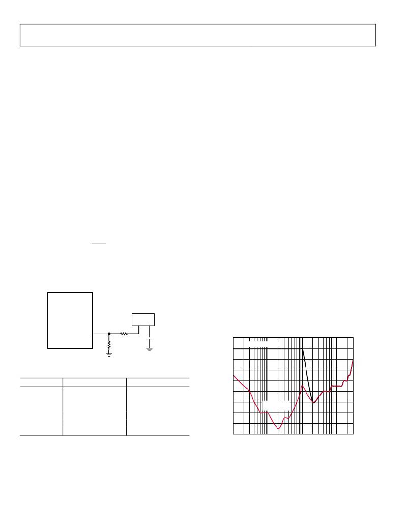
�PROGRAMMING� OUTPUT� VOLTAGE�
�ADP2302/ADP2303� have� an� adjustable� version� where� the� output�
�voltage� is� programmed� through� an� external� resistive� divider,� as�
�shown� in� Figure� 45.� Suggested� resistor� values� for� the� typical�
�output� voltage� setting� are� listed� in� Table� 6.� The� output� voltages�
�are� calculated� using� the� following� equation:�
�?� R� ?�
�?� R� BOT� ?�
�where:�
�V� OUT� is� the� output� voltage.�
�R� TOP� is� the� feedback� resistor� from� V� OUT� to� FB.�
�R� BOT� is� the� feedback� resistor� from� FB� to� GND.�
�Data� Sheet�
�for� the� worst� case.� By� considering� the� variation� of� both� the� switch-�
�ing� frequency� and� the� input� voltage,� the� equation� for� the� lower�
�limit� of� the� output� voltage� is�
�V� OUT(min)� =� t� MIN-ON� � f� SW(max)� � (� V� IN(max)� +� V� D� )� ?� V� D�
�where:�
�V� IN(max)� is� the� maximum� input� voltage.�
�f� SW(max� )� is� the� maximum� switching� frequency� for� the� worst� case.�
�t� MIN-ON� is� the� minimum� controllable� on� time.�
�V� D� is� the� diode� forward� drop.�
�The� upper� limit� of� the� output� voltage� is� constrained� by� the� mini-�
�mum� controllable� off� time,� which� can� be� as� high� as� 280� ns� in�
�ADP2302/ADP2303� for� the� worst� case.� By� considering� the�
�variation� of� both� the� switching� frequency� and� the� input� voltage,�
�the� equation� for� the� upper� limit� of� the� output� voltage� is�
�V� OUT(max)� =� (1� ?� t� MIN-OFF� � f� SW(max)� )� � (� V� IN(min)� +� V� D� )� ?� V� D�
�where:�
�V� IN(min)� is� the� minimum� input� voltage.�
�f� SW(max)� is� the� maximum� switching� frequency� for� the� worst� case.�
�V� D� is� the� diode� forward� drop.�
�t� MIN-OFF� is� the� minimum� controllable� off� time.�
�In� addition,� the� bootstrap� circuit� limits� the� minimum� input� voltage�
�for� the� desired� output� due� to� the� internal� dropout� voltage.� To�
�attain� stable� operation� at� light� loads� and� ensure� proper� startup� for�
�the� prebiased� condition,� the� ADP2302/ADP2303� require� the�
�voltage� difference� between� the� input� voltage� and� the� regulated�
�output� voltage� (or� between� the� input� voltage� and� the� prebias�
�voltage)� to� be� greater� than� 2.1� V� for� the� worst� case.� If� the� voltage�
�ADP2302/�
�ADP2303�
�FB�
�R� TOP�
�V� OUT�
�difference� is� smaller,� the� bootstrap� circuit� relies� on� some� minimum�
��shows� the� typical� required� minimum� input� voltage� vs.� load� current�
�for� the� 3.3� V� output� voltage.�
�5.3�
�R� BOT�
�Figure� 45.� Programming� the� Output� Voltage� Using� a� Resistive� Voltage� Divider�
�Table� 6.� Suggested� Values� for� Resistive� Voltage� Divider�
�5.1�
�4.9�
�4.7�
�FOR� START� UP�
�V� OUT� (V)�
�1.2�
�R� TOP� (kΩ),� ±1%�
�10�
�R� BOT� (kΩ),� ±1%�
�20�
�4.5�
�4.3�
�1.5�
�1.8�
�2.5�
�3.3�
�5.0�
�10�
�12.7�
�21.5�
�31.6�
�52.3�
�11.3�
�10.2�
�10.2�
�10.2�
�10�
�4.1�
�3.9�
�3.7�
�3.5�
�WHILE� IN�
�OPERATION�
�VOLTAGE� CONVERSION� LIMITATIONS�
�1�
�10� 100�
�OUPTUT� CURRENT� (mA)�
�1000�
�There� are� both� lower� and� upper� output� voltage� limitations� for� a�
�given� input� voltage� due� to� the� minimum� on� time,� the� minimum�
�off� time,� and� the� bootstrap� dropout� voltage.�
�The� lower� limit� of� the� output� voltage� is� constrained� by� the�
�Figure� 46.� Minimum� Input� Voltage� vs.� Load� Current�
�Based� on� three� conversion� limitations� (the� minimum� on� time,�
�the� minimum� off� time,� and� the� bootstrap� dropout� voltage),�
��controllable� minimum� on� time,� which� can� be� as� high� as� 170� ns�
�Rev.� A� |� Page� 16� of� 28�
�相关PDF资料 |
PDF描述 |
|---|---|
| MAX6855UK22D6+T | IC MPU SUPERVISOR SOT23-5 |
| ESC19DRTF-S13 | CONN EDGECARD 38POS .100 EXTEND |
| VI-B10-EU | CONVERTER MOD DC/DC 5V 200W |
| MAX6855UK22D3+T | IC MPU SUPERVISOR SOT23-5 |
| EMC19DRTF-S13 | CONN EDGECARD 38POS .100 EXTEND |
相关代理商/技术参数 |
参数描述 |
|---|---|
| ADP2303ARDZ-R7 | 功能描述:IC REG BUCK ADJ 3A 8SOIC RoHS:是 类别:集成电路 (IC) >> PMIC - 稳压器 - DC DC 开关稳压器 系列:- 产品培训模块:High Efficiency Current Mode Switching Regulators CMOS LDO Regulators 特色产品:BD91x Series Step-Down Regulators 标准包装:2,500 系列:- 类型:降压(降压) 输出类型:两者兼有 输出数:2 输出电压:3.3V,0.8 V ~ 2.5 V 输入电压:4.5 V ~ 5.5 V PWM 型:电流模式 频率 - 开关:1MHz 电流 - 输出:1.5A 同步整流器:是 工作温度:-40°C ~ 85°C 安装类型:表面贴装 封装/外壳:20-VFQFN 裸露焊盘 包装:带卷 (TR) 供应商设备封装:VQFN020V4040 产品目录页面:1373 (CN2011-ZH PDF) 其它名称:BD9152MUV-E2TR |
| ADP2303-EVALZ | 功能描述:EVAL BOARD FOR ADP2303 RoHS:是 类别:编程器,开发系统 >> 评估板 - DC/DC 与 AC/DC(离线)SMPS 系列:- 产品培训模块:Obsolescence Mitigation Program 标准包装:1 系列:True Shutdown™ 主要目的:DC/DC,步升 输出及类型:1,非隔离 功率 - 输出:- 输出电压:- 电流 - 输出:1A 输入电压:2.5 V ~ 5.5 V 稳压器拓扑结构:升压 频率 - 开关:3MHz 板类型:完全填充 已供物品:板 已用 IC / 零件:MAX8969 |
| ADP2303-EVALZ | 制造商:Analog Devices 功能描述:ADP2303, DC TO DC REGULATOR, STEP DOWN, |
| ADP2311-1-EVALZ | 功能描述:ADP2311 - DC/DC, Step Down 2, Non-Isolated Outputs Evaluation Board 制造商:analog devices inc. 系列:- 零件状态:有效 主要用途:DC/DC,步降 输出和类型:2,非隔离 功率 - 输出:- 电压 - 输出:1.2V,3.3V 电流 - 输出:1A,1A 电压 - 输入:4.5 V ~ 18 V 稳压器拓扑:降压 频率 - 开关:300kHz 板类型:完全填充 所含物品:板 使用的 IC/零件:ADP2311 标准包装:1 |
| ADP2311ACPZ-1-R7 | 功能描述:Buck Switching Regulator IC Positive Adjustable 0.6V 2 Output 1A 24-WFQFN Exposed Pad, CSP 制造商:analog devices inc. 系列:- 包装:剪切带(CT) 零件状态:有效 功能:降压 输出配置:正 拓扑:降压 输出类型:可调式 输出数:2 电压 - 输入(最小值):4.5V 电压 - 输入(最大值):18V 电压 - 输出(最小值/固定):0.6V 电压 - 输出(最大值):18V 电流 - 输出:1A 频率 - 开关:300kHz 同步整流器:是 工作温度:-40°C ~ 125°C (TJ) 安装类型:表面贴装 封装/外壳:24-WFQFN 裸露焊盘,CSP 供应商器件封装:24-LFCSP-WQ(4x4) 标准包装:1 |
发布紧急采购,3分钟左右您将得到回复。