- 您现在的位置:买卖IC网 > PDF目录14894 > ADP2503ACPZ-3.3-R7 (Analog Devices Inc)IC REG BUCK BST 3.3V .6A 10LFCSP PDF资料下载
参数资料
| 型号: | ADP2503ACPZ-3.3-R7 |
| 厂商: | Analog Devices Inc |
| 文件页数: | 5/16页 |
| 文件大小: | 0K |
| 描述: | IC REG BUCK BST 3.3V .6A 10LFCSP |
| 产品变化通告: | Reliability Change 27/Apr/2012 |
| 标准包装: | 1 |
| 类型: | 降压(降压),升压(升压) |
| 输出类型: | 固定 |
| 输出数: | 1 |
| 输出电压: | 3.3V |
| 输入电压: | 2.3 V ~ 5.5 V |
| PWM 型: | 电流模式 |
| 频率 - 开关: | 2.5MHz |
| 电流 - 输出: | 600mA |
| 同步整流器: | 是 |
| 工作温度: | -40°C ~ 85°C |
| 安装类型: | 表面贴装 |
| 封装/外壳: | 10-WFDFN 裸露焊盘,CSP |
| 包装: | 标准包装 |
| 供应商设备封装: | 10-LFCSP-WD(3x3) |
| 其它名称: | ADP2503ACPZ-3.3-R7DKR |
�� ��
��
��Data� Sheet�
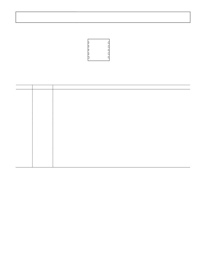
�PIN� CONFIGURATION� AND� FUNCTION� DESCRIPTIONS�
�ADP2503/ADP2504�
�VOUT� 1�
�ADP2503/�
�10� FB�
�SW2� 2�
�PGND� 3�
�SW1� 4�
�PVIN� 5�
�ADP2504�
�TOP� VIEW�
�(Not� to� scale)�
�9�
�8�
�7�
�6�
�AGND�
�VIN�
�SYNC�
�EN�
�NOTES�
�1.� CONNECT� EXPOSED� PAD� TO� PGND.�
�Figure� 2.� Pin� Configuration�
�Table� 4.� Pin� Function� Descriptions�
�Pin� No.�
�1�
�2�
�3�
�4�
�5�
�6�
�7�
�8�
�9�
�10�
�EP�
�Mnemonic�
�VOUT�
�SW2�
�PGND�
�SW1�
�PVIN�
�EN�
�SYNC�
�VIN�
�AGND�
�FB�
�Exposed� pad�
�Description�
�Output� of� the� ADP2503/ADP2504.� Connect� the� output� capacitor� between� VOUT� and� PGND.�
�Power� Switch� 2� Connection.� This� is� the� internal� connection� to� the� input� PMOS� and� NMOS� switches.� Connect�
�SW2� to� the� inductor� with� a� short,� wide� track.�
�Power� GND.� Connect� the� input� and� output� capacitors� and� the� PGND� pin� to� a� PGND� plane.�
�Power� Switch� 1� Connection.� This� is� the� internal� connection� to� the� output� PMOS� and� NMOS� switches.� Connect�
�SW1� to� the� inductor� with� a� short,� wide� track.�
�Power� Input.� This� the� input� to� the� buck-boost� power� switches.� Place� a� 10� μF� capacitor� between� PVIN� and�
�PGND� as� close� as� possible� to� the� ADP2503/ADP2504.�
�Enable.� Drive� EN� high� to� turn� on� the� ADP2503/ADP2504.� Bring� EN� low� to� put� the� part� into� shutdown� mode.�
�The� SYNC� pin� permits� the� ADP2503/ADP2504� to� operate� in� three� different� modes.�
�Normal� operation:� with� SYNC� driven� low,� the� ADP2503/ADP2504� operate� at� 2.5� MHz� PWM� mode� for� heavy�
�and� medium� loads,� and� moves� to� power� save� mode� (PSM)� mode� for� light� loads.�
�Forced� PWM� operation:� with� SYNC� driven� high,� the� ADP2503/ADP2504� operate� at� fixed� 2.5� MHz� PWM� mode�
�for� all� load� conditions.�
�SYNC� mode:� to� synchronize� the� ADP2503/ADP2504� switching� to� an� external� signal,� drive� this� pin� with� a� clock�
�between� 2.2� MHz� and� 2.8� MHz.� The� SYNC� signal� must� have� on� and� off� times� greater� than� 160� ns.�
�Analog� Power� Supply.� This� is� the� supply� for� the� ADP2503/ADP2504� internal� circuitry.�
�Analog� Ground.�
�Output� Feedback.� This� is� an� input� to� the� internal� error� amplifier� and� must� be� connected� to� VOUT� on� fixed�
�output� versions;� for� the� adjustable� model,� this� is� the� voltage� feedback.�
�Connect� the� exposed� pad� to� PGND.�
�Rev.� C� |� Page� 5� of� 16�
�相关PDF资料 |
PDF描述 |
|---|---|
| RBM24DCBN | CONN EDGECARD 48POS R/A .156 SLD |
| MAX6855UK27D6+T | IC MPU SUPERVISOR SOT23-5 |
| VI-B1M-EU | CONVERTER MOD DC/DC 10V 200W |
| RBM24DCBH | CONN EDGECARD 48POS R/A .156 SLD |
| RBM24DCBD | CONN EDGECARD 48POS R/A .156 SLD |
相关代理商/技术参数 |
参数描述 |
|---|---|
| ADP2503ACPZ-4.2-R7 | 功能描述:IC REG BUCK BST 4.2V .6A 10LFCSP RoHS:是 类别:集成电路 (IC) >> PMIC - 稳压器 - DC DC 开关稳压器 系列:- 标准包装:500 系列:- 类型:切换式电容器(充电泵),反相 输出类型:固定 输出数:1 输出电压:-3V 输入电压:2.3 V ~ 5.5 V PWM 型:Burst Mode? 频率 - 开关:900kHz 电流 - 输出:100mA 同步整流器:无 工作温度:-40°C ~ 85°C 安装类型:表面贴装 封装/外壳:SOT-23-6 细型,TSOT-23-6 包装:带卷 (TR) 供应商设备封装:TSOT-23-6 其它名称:LTC1983ES6-3#TRMTR |
| ADP2503ACPZ-4.2-R71 | 制造商:AD 制造商全称:Analog Devices 功能描述:600 mA/1000 mA, 2.5 MHz Buck-Boost DC-to-DC Converter |
| ADP2503ACPZ-4.5-R7 | 功能描述:IC REG BUCK BST 4.5V .6A 10LFCSP RoHS:是 类别:集成电路 (IC) >> PMIC - 稳压器 - DC DC 开关稳压器 系列:- 标准包装:500 系列:- 类型:切换式电容器(充电泵),反相 输出类型:固定 输出数:1 输出电压:-3V 输入电压:2.3 V ~ 5.5 V PWM 型:Burst Mode? 频率 - 开关:900kHz 电流 - 输出:100mA 同步整流器:无 工作温度:-40°C ~ 85°C 安装类型:表面贴装 封装/外壳:SOT-23-6 细型,TSOT-23-6 包装:带卷 (TR) 供应商设备封装:TSOT-23-6 其它名称:LTC1983ES6-3#TRMTR |
| ADP2503ACPZ-4.5-R71 | 制造商:AD 制造商全称:Analog Devices 功能描述:600 mA/1000 mA, 2.5 MHz Buck-Boost DC-to-DC Converter |
| ADP2503ACPZ-5.0-R7 | 功能描述:IC REG BUCK BST SYNC .6A 10LFCSP RoHS:是 类别:集成电路 (IC) >> PMIC - 稳压器 - DC DC 开关稳压器 系列:- 产品培训模块:Lead (SnPb) Finish for COTS Obsolescence Mitigation Program 标准包装:50 系列:- 类型:升压(升压) 输出类型:两者兼有 输出数:1 输出电压:5V,2 V ~ 16.5 V 输入电压:2 V ~ 16.5 V PWM 型:- 频率 - 开关:45kHz 电流 - 输出:50mA 同步整流器:无 工作温度:0°C ~ 70°C 安装类型:通孔 封装/外壳:8-DIP(0.300",7.62mm) 包装:管件 供应商设备封装:8-PDIP |
发布紧急采购,3分钟左右您将得到回复。