- 您现在的位置:买卖IC网 > PDF目录14203 > ADP2504ACPZ-2.8-R7 (Analog Devices Inc)IC REG BUCK BST SYNC 1A 10LFCSP PDF资料下载
参数资料
| 型号: | ADP2504ACPZ-2.8-R7 |
| 厂商: | Analog Devices Inc |
| 文件页数: | 13/16页 |
| 文件大小: | 0K |
| 描述: | IC REG BUCK BST SYNC 1A 10LFCSP |
| 产品变化通告: | Reliability Change 27/Apr/2012 |
| 标准包装: | 1 |
| 类型: | 降压(降压),升压(升压) |
| 输出类型: | 固定 |
| 输出数: | 1 |
| 输出电压: | 2.8V |
| 输入电压: | 2.3 V ~ 5.5 V |
| PWM 型: | 电流模式 |
| 频率 - 开关: | 2.5MHz |
| 电流 - 输出: | 1A |
| 同步整流器: | 是 |
| 工作温度: | -40°C ~ 85°C |
| 安装类型: | 表面贴装 |
| 封装/外壳: | 10-WFDFN 裸露焊盘,CSP |
| 包装: | 标准包装 |
| 供应商设备封装: | 10-LFCSP-WD(3x3) |
| 其它名称: | ADP2504ACPZ-2.8-R7DKR |
�� ��
��
��Data� Sheet�
�APPLICATIONS� INFORMATION�
�ADIsimPower� DESIGN� TOOL�
�The� ADP2503/ADP2504� is� supported� by� ADIsimPower� design�
�tool� set.� ADIsimPower� is� a� collection� of� tools� that� produce�
�complete� power� designs� optimized� for� a� specific� design� goal.�
�The� tools� enable� the� user� to� generate� a� full� schematic,� bill� of�
�materials,� and� calculate� performance� in� minutes.� ADIsimPower�
�can� optimize� designs� for� cost,� area,� efficiency,� and� parts� count�
�while� taking� into� consideration� the� operating� conditions� and�
�ADP2503/ADP2504�
�Ceramic� multilayer� inductors� can� be� used� with� lower� current�
�designs� for� a� reduced� overall� solution� size� and� dc� resistance�
�(DCR).� These� are� available� in� low� profile� packages.� Care� must�
�be� taken� because� these� derate� quickly� as� the� inductor� value� is�
�increased,� especially� at� higher� operating� temperatures.�
�Ferrite� core� inductors� have� good� core� loss� characteristics� as� well� as�
�reasonable� dc� resistance.� A� shielded� ferrite� inductor� reduces� the�
�EMI� generated� by� the� inductor.�
�limitations� of� the� IC� and� all� real� external� components.� For�
�more� information� about� ADIsimPower� design� tools,� refer� to�
�www.analog.com/ADIsimPower� .� The� tool� set� is� available� from�
�this� website,� and� users� can� also� request� an� unpopulated� board�
�through� the� tool.�
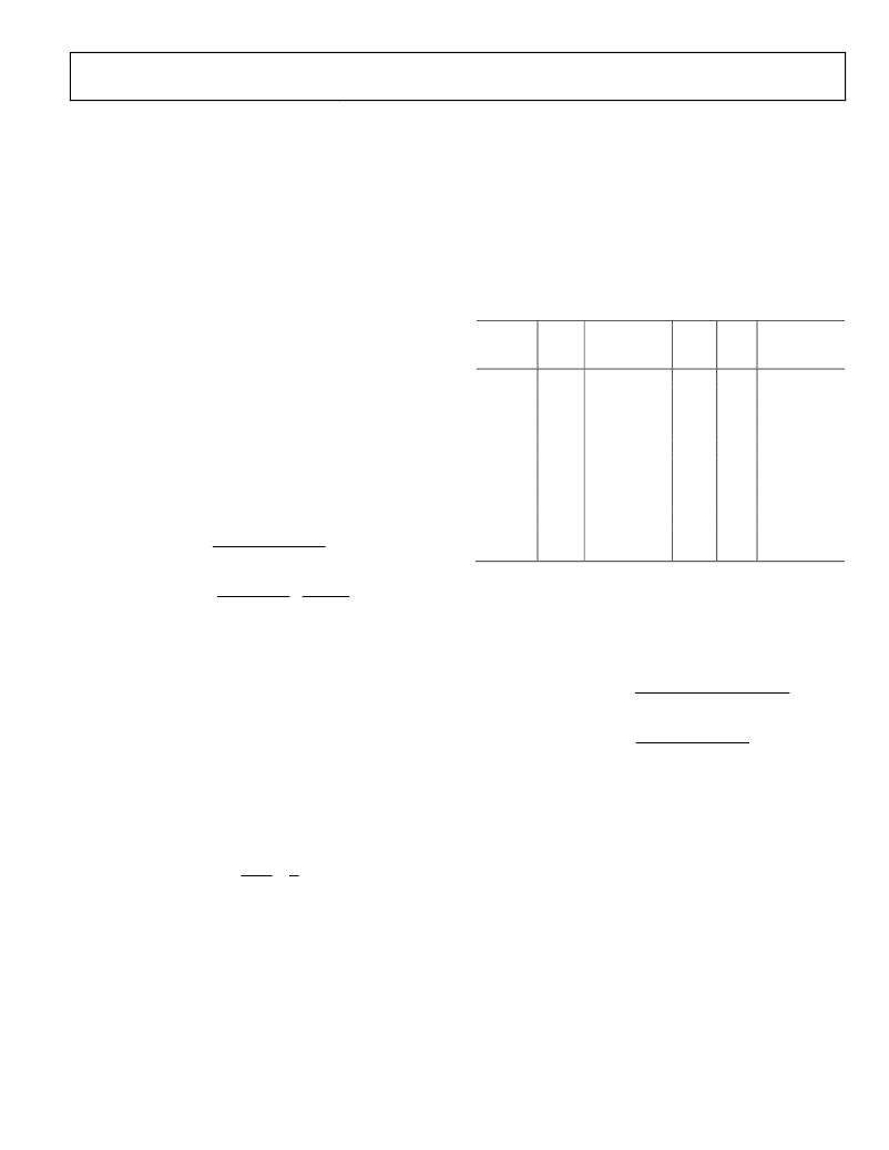
�Table� 5.� Sample� of� Recommended� Inductors�
�Value� DCR� I� SAT�
�Vendor� (μH)� Part� No.� (mΩ)� (A)�
�Toko� 1.2� DE2810C� 55� 1.7�
�Dimensions�
�L×W×� H�
�(mm)�
�2.8� � 2.8� � 1.0�
�V� OUT� � (� V� IN� ?� V� OUT� )�
�V� IN� � f� OSC� � L�
�INDUCTOR� SELECTION�
�The� high� 2.5� MHz� switching� frequency� of� the� ADP2503/�
�ADP2504� allows� for� minimal� output� voltage� ripple,� while�
�minimizing� inductor� size� and� cost.� Careful� inductor� selection�
�also� optimizes� efficiency� and� reduces� electromagnetic� interfe-�
�rence� (EMI).� The� selection� of� the� inductor� value� determines�
�the� inductor� current� ripple� and� loop� dynamics.�
�?� I� L� ,� peak� (� Buck� )� =�
�Toko�
�Toko�
�Murata�
�Murata�
�TDK�
�TDK�
�Coilcraft�
�Coilcraft�
�Taiyo�
�Yuden�
�1.5�
�1�
�1�
�1.5�
�1.0�
�1.5�
�1.0�
�1.5�
�1.5�
�DE2810C�
�MDT2520-CN�
�LQM2HP-G0�
�LQM2HP-G0�
�CPL2512T�
�CPL2512T�
�LPS3010�
�LPS3010�
�NR3015T1�
�60�
�100�
�55�
�70�
�90�
�120�
�85�
�120�
�40�
�1.5�
�1.8�
�1.6�
�1.5�
�1.5�
�1.2�
�1.7�
�1.3�
�1.5�
�2.8� � 2.8� � 1.0�
�2.5� � 2� � 1.2�
�2.5� � 2� � 1�
�2.5� � 2� � 1�
�2.5� � 1.5� � 1.2�
�2.5� � 1.5� � 1.2�
�3.0� � 3.0� � 0.9�
�3.0� � 3.0� � 0.9�
�3.0� � 3.0� � 1.5�
�(� V� OUT� ?� V� IN� )� V� IN�
�f� OSC� � L�
�?� I� L� ,� peak� (� Boost� )� =� �
�?� V� OUT� ,� peak� (� Buck� )� =�
�I� IN� (� MAX� )� =� I� LOAD� (� MAX� )� � ?� ?� OUT�
�?� V� ?� 1�
�?� η�
�?� V� OUT� ,� peak� (� Boost� )� =�
�V� OUT�
�where:�
�f� OSC� is� the� switching� frequency� (typically� 2.5� MHz).�
�L� is� the� inductor� value� in� henries.�
�A� larger� inductor� value� reduces� the� current� ripple� (and,� therefore,�
�the� peak� inductor� current),� but� is� physically� larger� in� size� with�
�increased� dc� resistance.� Inductor� values� between� 1� μH� and�
�1.5� μH� are� suggested.� The� maximum� inductor� value� to� ensure�
�stability� is� 2.0� μH.� For� increased� efficiency� with� the� ADP2504,�
�it� is� suggested� that� a� 1.5� μH� inductor� be� used.�
�The� inductor� peak� current� is� at� the� maximum� in� boost� mode.�
�To� determine� the� actual� maximum� inductor� current� in� boost�
�mode,� the� input� dc� current� should� be� estimated.�
�?� �
�?� V� IN� ?�
�where� η� is� efficiency� (assume� η� ≈� 0.85� to� 0.90).�
�The� saturation� current� rating� of� the� inductor� must� be� at� least�
�I� IN(MAX)� +� ΔI� LOAD� /2.�
�Output� Capacitor� Selection�
�The� output� capacitor� selection� determines� the� output� voltage�
�ripple,� transient� response,� and� the� loop� dynamics� of� the�
�ADP2503/ADP2504.� The� output� voltage� ripple� for� a� given�
�output� capacitor� is� as� follows:�
�V� OUT� � (� V� IN� ?� V� OUT� )�
�V� IN� � 8� � L� � (� f� OSC� )� 2� � C� OUT�
�I� LOAD� � (� V� OUT� ?� V� IN� )�
�C� OUT� � V� OUT� � f� OSC�
�If� the� ADP2503/ADP2504� are� operating� in� buck� mode,� the�
�worst-case� voltage� ripple� occurs� for� the� highest� input� voltage,�
�V� IN� .� If� the� ADP2503/ADP2504� are� operating� in� boost� mode,� the�
�worst-case� voltage� ripple� occurs� for� the� lowest� input� voltage,� V� IN� .�
�The� maximum� voltage� overshoot,� or� undershoot,� is� inversely�
�proportional� to� the� value� of� the� output� capacitor.� To� ensure�
�stability� and� excellent� transient� response,� it� is� recommended�
�to� use� a� minimum� of� 22� μF� X5R� 6.3� V� or� 2� ×� 10� μF� X5R� 6.3� V�
�capacitors� at� the� output.� The� effective� capacitance� (includes�
�temperature� and� dc� bias� effects)� needed� for� stability� is� 14� μF.�
�Rev.� C� |� Page� 13� of� 16�
�相关PDF资料 |
PDF描述 |
|---|---|
| MIC2571-2YMM TR | IC REG BOOST ADJ 1A 8MSOP |
| MIC2571-1YMM TR | IC REG BOOST 2.85V/3.3V/5V 8MSOP |
| VE-B1F-EW-F4 | CONVERTER MOD DC/DC 72V 100W |
| LM2575WT | IC REG BUCK ADJ 1A TO220-5 |
| VE-B1D-EX-F2 | CONVERTER MOD DC/DC 85V 75W |
相关代理商/技术参数 |
参数描述 |
|---|---|
| ADP2504ACPZ-3.3-R7 | 功能描述:IC REG BUCK BST SYNC 1A 10LFCSP RoHS:是 类别:集成电路 (IC) >> PMIC - 稳压器 - DC DC 开关稳压器 系列:- 产品培训模块:High Efficiency Current Mode Switching Regulators CMOS LDO Regulators 特色产品:BD91x Series Step-Down Regulators 标准包装:2,500 系列:- 类型:降压(降压) 输出类型:两者兼有 输出数:2 输出电压:3.3V,0.8 V ~ 2.5 V 输入电压:4.5 V ~ 5.5 V PWM 型:电流模式 频率 - 开关:1MHz 电流 - 输出:1.5A 同步整流器:是 工作温度:-40°C ~ 85°C 安装类型:表面贴装 封装/外壳:20-VFQFN 裸露焊盘 包装:带卷 (TR) 供应商设备封装:VQFN020V4040 产品目录页面:1373 (CN2011-ZH PDF) 其它名称:BD9152MUV-E2TR |
| ADP2504ACPZ-3.3-R71 | 制造商:AD 制造商全称:Analog Devices 功能描述:600 mA/1000 mA, 2.5 MHz Buck-Boost DC-to-DC Converter |
| ADP2504ACPZ-3.5-R7 | 功能描述:IC REG BUCK BST SYNC 1A 10LFCSP RoHS:是 类别:集成电路 (IC) >> PMIC - 稳压器 - DC DC 开关稳压器 系列:- 产品培训模块:Lead (SnPb) Finish for COTS Obsolescence Mitigation Program 标准包装:50 系列:- 类型:升压(升压) 输出类型:两者兼有 输出数:1 输出电压:5V,2 V ~ 16.5 V 输入电压:2 V ~ 16.5 V PWM 型:- 频率 - 开关:45kHz 电流 - 输出:50mA 同步整流器:无 工作温度:0°C ~ 70°C 安装类型:通孔 封装/外壳:8-DIP(0.300",7.62mm) 包装:管件 供应商设备封装:8-PDIP |
| ADP2504ACPZ-3.5-R71 | 制造商:AD 制造商全称:Analog Devices 功能描述:600 mA/1000 mA, 2.5 MHz Buck-Boost DC-to-DC Converter |
| ADP2504ACPZ-4.2-R7 | 功能描述:IC REG BUCK BST SYNC 1A 10LFCSP RoHS:是 类别:集成电路 (IC) >> PMIC - 稳压器 - DC DC 开关稳压器 系列:- 标准包装:500 系列:- 类型:切换式电容器(充电泵),反相 输出类型:固定 输出数:1 输出电压:-3V 输入电压:2.3 V ~ 5.5 V PWM 型:Burst Mode? 频率 - 开关:900kHz 电流 - 输出:100mA 同步整流器:无 工作温度:-40°C ~ 85°C 安装类型:表面贴装 封装/外壳:SOT-23-6 细型,TSOT-23-6 包装:带卷 (TR) 供应商设备封装:TSOT-23-6 其它名称:LTC1983ES6-3#TRMTR |
发布紧急采购,3分钟左右您将得到回复。