- 您现在的位置:买卖IC网 > PDF目录1778 > ADP3331ARTZ-REEL7 (Analog Devices Inc)IC REG LDO ADJ .2A SOT-23-6 PDF资料下载
参数资料
| 型号: | ADP3331ARTZ-REEL7 |
| 厂商: | Analog Devices Inc |
| 文件页数: | 8/9页 |
| 文件大小: | 0K |
| 描述: | IC REG LDO ADJ .2A SOT-23-6 |
| 标准包装: | 1 |
| 系列: | anyCAP® |
| 稳压器拓扑结构: | 正,可调式 |
| 输出电压: | 1.5 V ~ 11.75 V |
| 输入电压: | 2.6 V ~ 12 V |
| 电压 - 压降(标准): | 0.14V @ 200mA |
| 稳压器数量: | 1 |
| 电流 - 输出: | 200mA |
| 工作温度: | -40°C ~ 85°C |
| 安装类型: | 表面贴装 |
| 封装/外壳: | SOT-23-6 |
| 供应商设备封装: | SOT-23-6 |
| 包装: | 标准包装 |
| 产品目录页面: | 794 (CN2011-ZH PDF) |
| 其它名称: | ADP3331ARTZ-REEL7DKR |
�� �
�
�ADP3331�
�degree� of� overshoot� is� determined� by� several� factors:� the� output�
�voltage� setting,� the� output� load,� the� noise� reduction� capacitor,�
�and� the� output� capacitor.�
�SILICON�
�DIE�
�NORMAL� SOT-23-6� PACKAGE�
�SILICON� DIE�
�WITH�
�ELECTRICALLY�
�ISOLATED�
�DIE� ATTACH�
�THERMALLY� ENHANCED�
�CHIP-ON-LEAD� PACKAGE�
�The� output� voltage� setting� is� determined� by� the� application� and�
�cannot� be� tailored� for� minimum� overshoot.� In� general,� for� output�
�voltages� of� 2.2� V� or� less,� the� overshoot� becomes� larger� as� the�
�output� voltage� decreases.�
�The� output� load� is� also� determined� by� the� system� requirements.�
�P� D� =� (� V� IN� -� V� OUT� )� I� LOAD� +� (� V� IN� )� I� GND�
�Figure� 4.� Chip-on-Lead� Package�
�Calculating� Junction� Temperature�
�Device� power� dissipation� is� calculated� as� follows:�
�(8)�
�Where� I� LOAD� and� I� GND� are� load� current� and� ground� current� and�
�V� IN� and� V� OUT� are� the� input� and� output� voltages,� respectively.�
�Assuming� that� the� worst� case� operating� conditions� are� I� LOAD� =�
�200� mA,� I� GND� =� 4� mA,� V� IN� =� 4.2� V,� and� V� OUT� =� 3.0� V,� the�
�device� power� dissipation� is�
�P� D� =� (� 4� .� 2� V� -� 3� .� 0� V� )� 200� mA� +� (� 4� .� 2� V� )� 4� mA� =� 257� mW� (9)�
�The� proprietary� package� used� on� the� ADP3331� has� a� thermal�
�resistance� of� 165� ∞� C/W� when� placed� on� a� 4-layer� board� and�
�190� ∞� C/W� when� placed� on� a� 2-layer� board.� This� allows� the� ambient�
�temperature� to� be� significantly� higher� for� a� given� power� dissipa-�
�However,� if� the� ADP3331� has� no� load� on� the� output� during�
�startup,� a� small� amount� of� preload� can� be� added� to� minimize�
�overshoot.� A� preload� of� 2� m� A� to� 20� m� A� is� recommended.�
�A� noise� reduction� capacitor,� if� not� already� being� used,� is� sug-�
�gested� to� reduce� the� overshoot.� Values� in� the� range� of� 10� pF� to�
�100� pF� work� best,� along� with� the� preload� suggested� previously.�
�The� output� capacitor� can� be� adjusted� to� minimize� the� over-�
�shoot.� Values� in� the� 0.47� m� F� to� 1.0� m� F� range� should� be� used� in�
�conjunction� with� the� preload� and� noise� reduction� capacitor.�
�Further� increases� in� the� output� capacitance� may� be� acceptable� if�
�the� output� already� has� a� sizable� load� during� startup.�
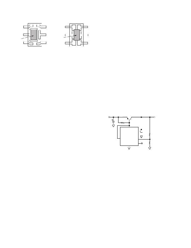
�Higher� Output� Current�
�The� ADP3331� can� source� up� to� 200� mA� without� any� heat� sink�
�or� pass� transistor.� If� higher� current� is� needed,� an� appropriate� pass�
�transistor� can� be� used,� as� in� Figure� 5,� to� increase� the� output�
�current� to� 1� A.�
�tion� than� with� a� standard� package.� Assuming� a� 4-layer� board,� the�
�junction� temperature� rise� above� ambient� will� be� approximately�
�equal� to�
�D� T� J� A� =� 0� .� 257� W� ¥� 165� o� C� /� W� =� 42� .� 4� o� C�
�(10)�
�V� IN� =� 3.3V�
�C1�
�47� F�
�R1�
�50�
�MJE253� *�
�IN�
�OUT�
�V� OUT� =� 1.8V� @� 1A�
�To� limit� the� junction� temperature� to� 125� ∞� C,� the� maximum�
�allowable� ambient� temperature� is�
�ADP3331�
�SD�
�FB�
�C2�
�10� F�
�340k�
�T� A� (� MAX� )� =� +� 125� o� C� -� 42� .� 4� o� C� =� 82� .� 6� o� C�
�(11)�
�GND�
�ERR�
�698k�
�Shutdown� Mode�
�Applying� a� TTL� level� high� signal� to� the� shutdown� (� SD� )� pin,� or�
�tying� it� to� the� input� pin,� will� turn� the� output� ON.� Pulling� the�
�SD� to� 0.4� V� or� below,� or� tying� it� to� ground,� will� turn� the� output�
�OFF.� In� shutdown� mode,� the� quiescent� current� is� reduced� to�
�less� than� 1� m� A.�
�Error� Flag� Dropout� Detector�
�The� ADP3331� will� maintain� its� output� voltage� over� a� wide�
�range� of� load,� input� voltage,� and� temperature� conditions.� If� the�
�output� is� about� to� lose� regulation� due� to� the� input� voltage�
�approaching� the� dropout� level,� the� error� flag� will� be� activated.�
�The� ERR� output� is� an� open� collector,� which� will� be� driven� low.�
�Once� set,� the� ERR� flag� ’� s� hysteresis� will� keep� the� output� low� until�
�a� small� margin� of� operating� range� is� restored� either� by� raising�
�the� supply� voltage� or� reducing� the� load.�
�Low� Voltage� Applications�
�In� applications� where� the� output� voltage� is� 2.2� V� or� less,� the�
�ADP3331� may� begin� to� exhibit� some� turn-on� overshoot.� The�
�–8� –�
�*� REQUIRES� HEAT� SINK�
�Figure� 5.� High� Output� Current� Linear� Regulator�
�Printed� Circuit� Board� Layout� Considerations�
�Use� the� following� general� guidelines� when� designing� printed�
�circuit� boards:�
�1.� PC� board� traces� with� larger� cross� sectional� areas� will� remove�
�more� heat� from� the� ADP3331.� For� optimum� heat� transfer,�
�specify� thick� copper� and� use� wide� traces.�
�2.� The� thermal� resistance� can� be� decreased� by� approximately�
�10%� by� adding� a� few� square� centimeters� of� copper� area� to�
�the� lands� connected� to� the� pins� of� the� LDO.�
�3.� The� feedback� pin� is� a� high� impedance� input,� and� care� should�
�be� taken� when� making� a� connection� to� this� pin.� The� voltage�
�setting� resistors� and� noise� reduction� network� must� be� located�
�as� close� as� possible.� Long� PC� board� traces� are� not� recom-�
�mended.� Avoid� routing� traces� near� possible� noise� sources.�
�REV.� B�
�相关PDF资料 |
PDF描述 |
|---|---|
| ADP3333ARMZ-5-R7 | IC REG LDO 5V .3A 8-MSOP |
| ADP3334ARMZ-REEL | IC REG LDO ADJ .5A 8MSOP |
| ADP3335ARMZ-2.5-RL | IC REG LDO 2.5V .5A 8-MSOP |
| ADP3336ARMZ-REEL7 | IC REG LDO ADJ .5A 8-MSOP |
| ADP3338AKCZ-5-REEL | IC REG LDO 5V 1A SOT223 |
相关代理商/技术参数 |
参数描述 |
|---|---|
| ADP3331ARTZ-REEL7 | 制造商:Analog Devices 功能描述:Linear Voltage Regulator IC 制造商:Analog Devices 功能描述:IC, ADJ LDO REG, 1.5V TO 11.75V, SOT23-6 |
| ADP3333 | 制造商:AD 制造商全称:Analog Devices 功能描述:High Accuracy Ultralow IQ, 300 mA, anyCAP Low Dropout Regulator |
| ADP3333_09 | 制造商:AD 制造商全称:Analog Devices 功能描述:High Accuracy Ultralow IQ, 300 mA, anyCAP Low Dropout Regulator |
| ADP3333ARM-1.5 | 制造商:未知厂家 制造商全称:未知厂家 功能描述:Analog IC |
| ADP3333ARM-1.5-RL | 制造商:Analog Devices 功能描述:LDO Regulator Pos 1.5V 0.6A 8-Pin MSOP T/R |
发布紧急采购,3分钟左右您将得到回复。