- 您现在的位置:买卖IC网 > PDF目录165353 > ADP3335ARMZ-1.8RL7 (ANALOG DEVICES INC) 1.8 V FIXED POSITIVE LDO REGULATOR, 0.37 V DROPOUT, PDSO8 PDF资料下载
参数资料
| 型号: | ADP3335ARMZ-1.8RL7 |
| 厂商: | ANALOG DEVICES INC |
| 元件分类: | 固定正电压单路输出LDO稳压器 |
| 英文描述: | 1.8 V FIXED POSITIVE LDO REGULATOR, 0.37 V DROPOUT, PDSO8 |
| 封装: | MO-187AA, MSOP-8 |
| 文件页数: | 3/16页 |
| 文件大小: | 442K |
| 代理商: | ADP3335ARMZ-1.8RL7 |
ADP3335
Rev. A | Page 11 of 16
PRINTED CIRCUIT BOARD LAYOUT
CONSIDERATIONS
All surface-mount packages rely on the traces of the PC board
to conduct heat away from the package. Use the following
general guidelines when designing printed circuit boards to
improve both electrical and thermal performance.
1.
Keep the output capacitor as close as possible to the output
and ground pins.
2.
Keep the input capacitor as close as possible to the input
and ground pins.
3.
PC board traces with larger cross sectional areas will
remove more heat from the ADP3335. For optimum heat
transfer, specify thick copper and use wide traces.
4.
It is not recommended to use solder mask or silkscreen on
the PCB traces adjacent to the ADP3335’s pins, since doing
so will increase the junction-to-ambient thermal resistance
of the package.
5.
Use additional copper layers or planes to reduce the
thermal resistance. When connecting to other layers, use
multiple vias, if possible.
LFCSP LAYOUT CONSIDERATIONS
The LFCSP package has an exposed die paddle on the bottom,
which efficiently conducts heat to the PCB. In order to achieve
the optimum performance from the LFCSP package, special
consideration must be given to the layout of the PCB. Use the
following layout guidelines for the LFCSP package.
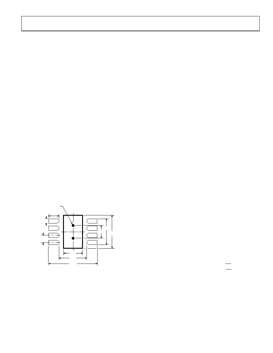
0.50
2
× VIAS, 0.250
35
m PLATING
3.36
0.90
1.80
2.36
1.90
1.40
0.30
0.73
00147-0-024
Figure 25. 3 mm × 3 mm LFCSP Pad Pattern
(Dimensions shown in millimeters)
1.
The pad pattern is given in Figure 25. The pad dimension
should be followed closely for reliable solder joints, while
maintaining reasonable clearances to prevent solder
bridging.
2.
The thermal pad of the LFCSP package provides a low
thermal impedance path (approximately 20°C/W) to the
PCB. Therefore, the PCB must be properly designed to
effectively conduct heat away from the package. This is
achieved by adding thermal vias to the PCB, which provide
a thermal path to the inner or bottom layers. See Figure 25
for the recommended via pattern. Note that the via
diameter is small to prevent the solder from flowing
through the via and leaving voids in the thermal pad solder
joint.
Also, note that the thermal pad is attached to the die
substrate, so the thermal planes to which the thermal vias
connect must be electrically isolated or tied to VIN. Do
NOT connect the thermal pad to ground.
3.
The solder mask opening should be about 120 (4.7 mils)
larger than the pad size, resulting in a minimum 60 m
(2.4 mils) clearance between the pad and the solder mask.
4.
The paste mask opening is typically designed to match the
pad size used on the peripheral pads of the LFCSP package.
This should provide a reliable solder joint as long as the
stencil thickness is about 0.125 mm. The paste mask for the
thermal pad needs to be designed for the maximum
coverage to effectively remove the heat from the package.
However, due to the presence of thermal vias and the size
of the thermal pad, eliminating voids may not be possible.
5.
The recommended paste mask stencil thickness is
0.125 mm. A laser cut stainless steel stencil with
trapezoidal walls should be used. A “No Clean” Type 3
solder paste should be used for mounting the LFCSP
package. Also, a nitrogen purge during the reflow process is
recommended.
6.
The package manufacturer recommends that the reflow
temperature should not exceed 220°C and the time above
liquidus is less than 75 seconds. The preheat ramp should
be 3°C/second or lower. The actual temperature profile
depends on the board density and must be determined by
the assembly house as to what works best.
SHUTDOWN MODE
Applying a TTL high signal to the shutdown (SD) pin or tying it
to the input pin, turns the output ON. Pulling SD down to 0.4 V
or below, or tying it to ground, turns the output OFF. In shut-
down mode, quiescent current is reduced to a typical value of
10 nA.
相关PDF资料 |
PDF描述 |
|---|---|
| ADP3335ARMZ-5-REEL7 | 5 V FIXED POSITIVE LDO REGULATOR, 0.37 V DROPOUT, PDSO8 |
| ADP5024ACPZ-1-R7 | SWITCHING REGULATOR, PQCC24 |
| ADPDF5A24AC | SNAP ACTING/LIMIT SWITCH, DPDT, MOMENTARY, 1A, 30VDC, 12mm, PANEL MOUNT |
| ADPDF5P04AW | SNAP ACTING/LIMIT SWITCH, DPST, MOMENTARY, 1A, 30VDC, 2.54mm, PANEL MOUNT |
| ADPFF5W04AC | SNAP ACTING/LIMIT SWITCH, DPDT, MOMENTARY, 1A, 30VDC, 8.71mm, PANEL MOUNT |
相关代理商/技术参数 |
参数描述 |
|---|---|
| ADP3335ARMZ-2.5-RL | 功能描述:IC REG LDO 2.5V .5A 8-MSOP RoHS:是 类别:集成电路 (IC) >> PMIC - 稳压器 - 线性 系列:anyCAP® 标准包装:1 系列:anyCAP® 稳压器拓扑结构:正,固定式 输出电压:3.3V 输入电压:最高 6V 电压 - 压降(标准):0.23V @ 1.5A 稳压器数量:1 电流 - 输出:1.5A 电流 - 限制(最小):- 工作温度:-40°C ~ 85°C 安装类型:表面贴装 封装/外壳:TO-261-4,TO-261AA 供应商设备封装:SOT-223-3 包装:Digi-Reel® 其它名称:ADP3339AKCZ-3.3-RLDKR |
| ADP3335ARMZ-2.5RL7 | 功能描述:IC REG LDO 2.5V .5A 8-MSOP RoHS:是 类别:集成电路 (IC) >> PMIC - 稳压器 - 线性 系列:anyCAP® 标准包装:1 系列:- 稳压器拓扑结构:正,固定式 输出电压:8V 输入电压:10.5 V ~ 23 V 电压 - 压降(标准):1.7V @ 40mA 稳压器数量:1 电流 - 输出:100mA(最小值) 电流 - 限制(最小):- 工作温度:0°C ~ 125°C 安装类型:表面贴装 封装/外壳:8-SOIC(0.154",3.90mm 宽) 供应商设备封装:8-SOIC 包装:剪切带 (CT) 产品目录页面:1075 (CN2011-ZH PDF) 其它名称:296-24390-1 |
| ADP3335ARMZ-2.85R7 | 功能描述:IC REG LDO 2.85V .5A 8-MSOP RoHS:是 类别:集成电路 (IC) >> PMIC - 稳压器 - 线性 系列:anyCAP® 标准包装:1 系列:- 稳压器拓扑结构:正,固定式 输出电压:3.3V 输入电压:2.5 V ~ 5.5 V 电压 - 压降(标准):0.1V @ 200mA 稳压器数量:2 电流 - 输出:300mA 电流 - 限制(最小):350mA 工作温度:-40°C ~ 85°C 安装类型:表面贴装 封装/外壳:8-UFQFN 供应商设备封装:8-MLPQ-UT(1.5x1.5) 包装:剪切带 (CT) 产品目录页面:1358 (CN2011-ZH PDF) 其它名称:SC560HULCT |
| ADP3335ARMZ-2.85RL | 功能描述:IC REG LDO 2.85V .5A 8MSOP RoHS:是 类别:集成电路 (IC) >> PMIC - 稳压器 - 线性 系列:anyCAP® 标准包装:1 系列:- 稳压器拓扑结构:正,固定式 输出电压:2.7V 输入电压:最高 5.5V 电压 - 压降(标准):0.21V @ 150mA 稳压器数量:1 电流 - 输出:150mA 电流 - 限制(最小):- 工作温度:-40°C ~ 125°C 安装类型:表面贴装 封装/外壳:SOT-23-5 细型,TSOT-23-5 供应商设备封装:TSOT-23-5 包装:剪切带 (CT) 产品目录页面:1100 (CN2011-ZH PDF) 其它名称:576-1852-1 |
| ADP3335ARMZ-3.3 | 制造商:Analog Devices 功能描述:LDO 3.3V 500MA 8-MSOP 制造商:Analog Devices 功能描述:LDO, 3.3V, 500MA, 8-MSOP 制造商:Analog Devices 功能描述:LDO, 3.3V, 500MA, 8-MSOP, Primary Input Voltage:12V, Output Voltage Fixed:3.3V, 制造商:Analog Devices 功能描述:LDO, 3.3V, 500MA, 8-MSOP, Primary Input Voltage:12V, Output Voltage Fixed:3.3V, Dropout Voltage Vdo:200mV, Voltage Regulator Case Style:MSOP, No. of Pins:8, Output Current:500mA, Operating Temperature Min:-40C, Operating Temperature, RoHS Compliant: Yes |
发布紧急采购,3分钟左右您将得到回复。