- 您现在的位置:买卖IC网 > PDF目录13140 > ADP3335ARMZ-5-REEL (Analog Devices Inc)IC REG LDO 5V .5A 8MSOP PDF资料下载
参数资料
| 型号: | ADP3335ARMZ-5-REEL |
| 厂商: | Analog Devices Inc |
| 文件页数: | 10/16页 |
| 文件大小: | 0K |
| 描述: | IC REG LDO 5V .5A 8MSOP |
| 标准包装: | 1 |
| 系列: | anyCAP® |
| 稳压器拓扑结构: | 正,固定式 |
| 输出电压: | 5V |
| 输入电压: | 最高 12V |
| 电压 - 压降(标准): | 0.2V @ 500mA |
| 稳压器数量: | 1 |
| 电流 - 输出: | 500mA |
| 工作温度: | -40°C ~ 85°C |
| 安装类型: | 表面贴装 |
| 封装/外壳: | 8-TSSOP,8-MSOP(0.118",3.00mm 宽) |
| 供应商设备封装: | 8-MSOP |
| 包装: | 标准包装 |
| 其它名称: | ADP3335ARMZ-5-REELDKR |
�� ��
��
��ADP3335�
�APPLICATIONS� INFORMATION�
�OUTPUT� CAPACITOR� SELECTION�
�As� with� any� micropower� device,� output� transient� response� is� a�
�function� of� the� output� capacitance.� The� ADP3335� is� stable� over�
�a� wide� range� of� capacitor� values,� types,� and� ESR� (anyCAP).� A�
�capacitor� as� low� as� 1� μF� is� all� that� is� needed� for� stability;� larger�
�capacitors� can� be� used� if� high� output� current� surges� are� anticipated.�
�The� ADP3335� is� stable� with� extremely� low� ESR� capacitors� (ESR�
�≈� 0),� such� as� multilayer� ceramic� capacitors� (MLCC)� or� organic�
�semiconductor� electrolytic� capacitors� (OSCON).� Note� that� the�
�effective� capacitance� of� some� capacitor� types� may� fall� below� the�
�minimum� at� extreme� temperatures.� Ensure� that� the� capacitor�
�provides� more� than� 1� μF� over� the� entire� temperature� range.�
�INPUT� BYPASS� CAPACITOR�
�An� input� bypass� capacitor� is� not� strictly� required,� but� is� advisable�
�in� any� application� involving� long� input� wires� or� high� source�
�impedance.� Connecting� a� 1� μF� capacitor� from� IN� to� ground�
�reduces� the� circuit’s� sensitivity� to� PC� board� layout.� If� a� larger�
�value� output� capacitor� is� used,� then� a� larger� value� input� capacitor�
�is� also� recommended.�
�NOISE� REDUCTION�
�A� noise� reduction� capacitor� (C� NR� )� can� be� used,� as� shown� in�
��Low� leakage� capacitors� in� the� 100� pF� to� 1� nF� range� provide� the� best�
�performance.� Since� the� noise� reduction� pin,� NR,� is� internally�
�connected� to� a� high� impedance� node,� any� connection� to� this� node�
�should� be� made� carefully� to� avoid� noise� pickup� from� external�
�sources.� The� pad� connected� to� this� pin� should� be� as� small� as�
�possible,� and� long� PC� board� traces� are� not� recommended.�
�When� adding� a� noise� reduction� capacitor,� maintain� a� minimum�
�load� current� of� 1� mA� when� not� in� shutdown.�
�It� is� important� to� note� that� as� C� NR� increases,� the� turn-on� time�
�will� be� delayed.� With� NR� values� greater� than� 1� nF,� this� delay�
�may� be� on� the� order� of� several� milliseconds.�
�C� NR�
�5�
�Data� Sheet�
�THERMAL� OVERLOAD� PROTECTION�
�The� ADP3335� is� protected� against� damage� from� excessive�
�power� dissipation� by� its� thermal� overload� protection� circuit,�
�which� limits� the� die� temperature� to� a� maximum� of� 165°C.�
�Under� extreme� conditions� (i.e.,� high� ambient� temperature� and�
�power� dissipation)� where� die� temperature� starts� to� rise� above�
�165°C,� the� output� current� is� reduced� until� the� die� temperature�
�has� dropped� to� a� safe� level.� The� output� current� is� restored� when�
�the� die� temperature� is� reduced.�
�Current� and� thermal� limit� protections� are� intended� to� protect�
�the� device� against� accidental� overload� conditions.� For� normal�
�operation,� device� power� dissipation� should� be� externally� limited�
�so� that� junction� temperatures� will� not� exceed� 150°C.�
�CALCULATING� JUNCTION� TEMPERATURE�
�Device� power� dissipation� is� calculated� as� follows:�
�P� D� =� (� V� IN� ?� V� OUT� )� I� LOAD� +� (� V� IN� )� I� GND�
�Where� I� LOAD� and� I� GND� are� load� current� and� ground� current,� and�
�V� IN� and� V� OUT� are� input� and� output� voltages,� respectively.�
�Assuming� I� LOAD� =� 400� mA,� I� GND� =� 4� mA,� V� IN� =� 5.0� V,� and� V� OUT� =�
�3.3� V,� device� power� dissipation� is�
�P� D� =� (5� V� –� 3.3� V)400� mA� +� 5.0� V(4� mA)� =� 700� mW�
�The� junction� temperature� can� be� calculated� from� the� power�
�dissipation,� ambient� temperature,� and� package� thermal� resistance.�
�The� thermal� resistance� is� a� function� not� only� of� the� package,� but�
�also� of� the� circuit� board� layout.� Standard� test� conditions� are� used� to�
�determine� the� values� published� in� this� data� sheet,� but� actual�
�performance� will� vary.� For� an� LFCSP-8� package� mounted� on� a�
�standard� 4-layer� board,� θ� JA� is� 48°C/W.� In� the� above� example,� where�
�the� power� dissipation� is� 700� mW,� the� temperature� rise� above�
�ambient� will� be� approximately� equal� to�
�?� T� JA� =� 0.700� W� ×� 48°C/W� =� 33.6°C�
�To� limit� the� maximum� junction� temperature� to� 150°C,� the�
�maximum� allowable� ambient� temperature� will� be�
�T� AMAX� =� 150°C� ?� 33.6°C� =� 116.4°C�
�7�
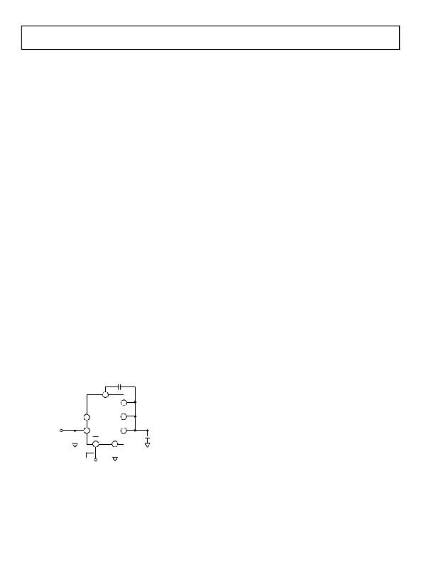
�NR� OUT� 3�
�ADP3335�
�IN� OUT� 2�
�In� this� case,� the� resulting� ambient� temperature� limitation� is�
�above� the� maximum� allowable� ambient� temperature� of� 85°C.�
�V� IN�
�C� IN�
�1� μ� F�
�+�
�8�
�IN�
�SD�
�6�
�OUT� 1�
�GND�
�4�
�+�
�V� OUT�
�C� OUT�
�1� μ� F�
�ON�
�OFF�
�Figure� 24.� Typical� Application� Circuit�
�Rev.� D� |� Page� 10� of� 16�
�相关PDF资料 |
PDF描述 |
|---|---|
| GMC25DRTN-S734 | CONN EDGECARD 50POS DIP .100 SLD |
| VI-B6P-EU | CONVERTER MOD DC/DC 13.8V 200W |
| UPM1V151MPD6 | CAP ALUM 150UF 35V 20% RADIAL |
| 420BXW100MEFC16X35 | CAP ALUM 100UF 420V 20% RADIAL |
| EMM15DRUS | CONN EDGECARD 30POS DIP .156 SLD |
相关代理商/技术参数 |
参数描述 |
|---|---|
| ADP3336 | 制造商:AD 制造商全称:Analog Devices 功能描述:High Accuracy Ultralow IQ, 500 mA anyCAP Adjustable Low Dropout Regulator |
| ADP3336ARM-REEL | 制造商:Analog Devices 功能描述:LDO Regulator Pos 1.5V to 10V 0.8A 8-Pin MSOP T/R |
| ADP3336ARM-REEL7 | 功能描述:IC REG LDO ADJ .5A 8-MSOP RoHS:否 类别:集成电路 (IC) >> PMIC - 稳压器 - 线性 系列:anyCAP® 标准包装:3,000 系列:- 稳压器拓扑结构:正,固定式和可调式 输出电压:3.3V,1.25 V ~ 5.7 V 输入电压:4.5 V ~ 7 V 电压 - 压降(标准):1.1V @ 1A 稳压器数量:2 电流 - 输出:1A 电流 - 限制(最小):1A 工作温度:0°C ~ 125°C 安装类型:表面贴装 封装/外壳:TO-252-5,DPak(4 引线 + 接片),TO-252AD 供应商设备封装:PPAK 包装:管件 其它名称:497-3576-5 |
| ADP3336ARMZ | 制造商:Analog Devices 功能描述:LDO 2.6-12V 0.5A 1.5-10V 8 制造商:Analog Devices 功能描述:LDO, 2.6-12V, 0.5A, 1.5-10V, 8MSOP; Primary Input Voltage:12V; Dropout Voltage Vdo:200mV; Voltage Regulator Case Style:MSOP; No. of Pins:8; Output Current:500mA; Operating Temperature Min:-40C; Operating Temperature Max:85C; MSL:-;;RoHS Compliant: Yes |
| ADP3336ARMZ-REEL | 制造商:Analog Devices 功能描述:LDO Regulator Pos 1.5V to 10V 0.8A 8-Pin MSOP T/R 制造商:Analog Devices 功能描述:LDO ADJ 0.5A SMD MSOP8 3336 |
发布紧急采购,3分钟左右您将得到回复。