- 您现在的位置:买卖IC网 > PDF目录13080 > ADP3339AKCZ-3-RL7 (Analog Devices Inc)IC REG LDO 3V 1.5A SOT-223 PDF资料下载
参数资料
| 型号: | ADP3339AKCZ-3-RL7 |
| 厂商: | Analog Devices Inc |
| 文件页数: | 10/12页 |
| 文件大小: | 0K |
| 描述: | IC REG LDO 3V 1.5A SOT-223 |
| 标准包装: | 1 |
| 系列: | anyCAP® |
| 稳压器拓扑结构: | 正,固定式 |
| 输出电压: | 3V |
| 输入电压: | 最高 6V |
| 电压 - 压降(标准): | 0.23V @ 1.5A |
| 稳压器数量: | 1 |
| 电流 - 输出: | 1.5A |
| 工作温度: | -40°C ~ 85°C |
| 安装类型: | 表面贴装 |
| 封装/外壳: | TO-261-4,TO-261AA |
| 供应商设备封装: | SOT-223-3 |
| 包装: | 标准包装 |
| 产品目录页面: | 794 (CN2011-ZH PDF) |
| 其它名称: | ADP3339AKCZ-3-RL7DKR |
�� ��
��
��ADP3339�
�APPLICATIONS� INFORMATION�
�CAPACITOR� SELECTION�
�Output� Capacitor�
�Data� Sheet�
�Therefore,� for� a� junction� temperature� of� 125°C� and� a� maximum�
�ambient� temperature� of� 85°C,� the� required� thermal� resistance�
�from� junction� to� ambient� is�
�The� stability� and� transient� response� of� the� LDO� is� a� function� of�
�the� output� capacitor.� The� ADP3339� is� stable� with� a� wide� range�
�of� capacitor� values,� types,� and� ESR� (anyCAP).� A� capacitor� as� low� as�
�θ� JA� =�
�125� °� C� ?� 85� °� C�
�1� .� 246� W�
�=� 32� .� 1� °� C/W�
�1� μF� is� all� that� is� needed� for� stability.� A� higher� capacitance� may�
�be� necessary� if� high� output� current� surges� are� anticipated,� or� if�
�the� output� capacitor� cannot� be� located� near� the� output� and�
�ground� pins.� The� ADP3339� is� stable� with� extremely� low� ESR�
�capacitors� (ESR� ≈� 0)� such� as� multilayer� ceramic� capacitors�
�(MLCC)� or� OSCON.� Note� that� the� effective� capacitance� of�
�some� capacitor� types� falls� below� the� minimum� over� tempera-�
�ture� or� with� dc� voltage.�
�Input� Capacitor�
�An� input� bypass� capacitor� is� not� strictly� required� but� is� recom-�
�mended� in� any� application� involving� long� input� wires� or� high�
�source� impedance.� Connecting� a� 1� μF� capacitor� from� the� input�
�to� ground� reduces� the� circuit’s� sensitivity� to� PC� board� layout�
�and� input� transients.� If� a� larger� output� capacitor� is� necessary,� a�
�larger� value� input� capacitor� is� also� recommended.�
�OUTPUT� CURRENT� LIMIT�
�The� ADP3339� is� short-circuit� protected� by� limiting� the� pass�
�transistor’s� base� drive� current.� The� maximum� output� current� is�
��THERMAL� OVERLOAD� PROTECTION�
�PRINTED� CIRCUIT� BOARD� LAYOUT�
�CONSIDERATIONS�
�The� thermal� resistance,� θ� JA� ,� of� SOT-223� is� determined� by� the�
�sum� of� the� junction-to-case� and� the� case-to-ambient� thermal�
�resistances.� The� junction-to-case� thermal� resistance,� θ� JC� ,� is�
�determined� by� the� package� design� and� specified� at� 26.8°C/W.�
�However,� the� case-to-ambient� thermal� resistance� is� determined�
�by� the� printed� circuit� board� design.�
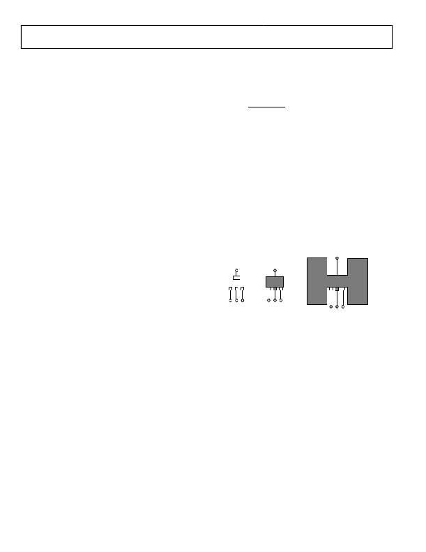
�As� shown� in� Figure� 22,� the� amount� of� copper� onto� which� the�
�ADP3339� is� mounted� affects� thermal� performance.� When�
�mounted� onto� the� minimal� pads� of� 2� oz.� copper� (see� Figure� 22a),�
�θ� JA� is� 126.6°C/W.� Adding� a� small� copper� pad� under� the�
�ADP3339� (see� Figure� 22b)� reduces� the� θ� JA� to� 102.9°C/W.�
�Increasing� the� copper� pad� to� 1� square� inch� (see� Figure� 22c)�
�reduces� the� θ� JA� even� further,� to� 52.8°C/W.�
�The� ADP3339� is� protected� against� damage� due� to� excessive� power�
�dissipation� by� its� thermal� overload� protection� circuit.� Thermal�
�a�
�b�
�c�
�protection� limits� the� die� temperature� to� a� maximum� of� 160°C.�
�Under� extreme� conditions� (that� is,� high� ambient� temperature�
�and� power� dissipation)� where� the� die� temperature� starts� to� rise�
�Figure� 22.� PCB� Layouts�
�Use� the� following� general� guidelines� when� designing� printed�
�circuit� boards:�
�above� 160°C,� the� output� current� is� reduced� until� the� die� tempera-�
�ture� has� dropped� to� a� safe� level.�
�Current� and� thermal� limit� protections� are� intended� to� protect�
�the� device� against� accidental� overload� conditions.� For� normal�
�operation,� the� device’s� power� dissipation� should� be� externally�
�limited� so� that� the� junction� temperature� does� not� exceed� 150°C.�
�CALCULATING� POWER� DISSIPATION�
�Device� power� dissipation� is� calculated� as� follows:�
�P� D� =� (� V� IN� –� V� OUT� )� ×� I� LOAD� +� (� V� IN� ×� I� GND� )�
�where� I� LOAD� and� I� GND� are� the� load� current� and� ground� current,�
�and� V� IN� and� V� OUT� are� the� input� and� output� voltages,� respectively.�
�Assuming� worst-case� operating� conditions� are� I� LOAD� =� 1.5� A,�
�I� GND� =� 14� mA,� V� IN� =� 3.3� V,� and� V� OUT� =� 2.5� V,� the� device� power�
�dissipation� is�
�P� D� =� (3.3� V� –� 2.5� V)� ×� 1500� mA� +� (3.3� V� ×� 14� mA)� =� 1246� mW�
�1.�
�2.�
�3.�
�4.�
�5.�
�6.�
�Keep� the� output� capacitor� as� close� to� the� output� and�
�ground� pins� as� possible.�
�Keep� the� input� capacitor� as� close� to� the� input� and� ground�
�pins� as� possible.�
�PC� board� traces� with� larger� cross� sectional� areas� remove�
�more� heat� from� the� ADP3339.� For� optimum� heat� transfer,�
�use� thick� copper� and� use� wide� traces.�
�The� thermal� resistance� can� be� decreased� by� adding� a�
�copper� pad� under� the� ADP3339,� as� shown� in� Figure� 22b.�
�If� possible,� use� the� adjacent� area� to� add� more� copper�
�around� the� ADP3339.� Connecting� the� copper� area� to� the�
�output� of� the� ADP3339,� as� shown� in� Figure� 22c,� is� best,� but�
�thermal� performance� is� improved� even� if� it� is� connected� to�
�other� pins.�
�Use� additional� copper� layers� or� planes� to� reduce� the�
�thermal� resistance.� Again,� connecting� the� other� layers� to�
�the� output� of� the� ADP3339� is� best,� but� is� not� necessary.�
�When� connecting� the� output� pad� to� other� layers,� use�
�multiple� vias.�
�Rev.� C� |� Page� 10� of� 12�
�相关PDF资料 |
PDF描述 |
|---|---|
| VI-JWD-EZ-B1 | CONVERTER MOD DC/DC 85V 25W |
| 450VXH150MEFCSN22X35 | CAP ALUM 150UF 450V 20% SNAP-IN |
| ABC08DRYH-S13 | CONN EDGECARD 16POS .100 EXTEND |
| EMK212B7474KD-T | CAP CER 0.47UF 16V 10% X7R 0805 |
| 63MXG3900MEFCSN25X30 | CAP ALUM 3900UF 63V 20% SNAP-IN |
相关代理商/技术参数 |
参数描述 |
|---|---|
| ADP3339AKCZ-5-R7 | 功能描述:IC REG LDO 5V 1.5A SOT-223 RoHS:是 类别:集成电路 (IC) >> PMIC - 稳压器 - 线性 系列:anyCAP® 产品培训模块:MIC5365/66 Ultra-small LDO Regulators 标准包装:1 系列:- 稳压器拓扑结构:正,固定式 输出电压:3V 输入电压:最高 5.5V 电压 - 压降(标准):0.155V @ 150mA 稳压器数量:1 电流 - 输出:150mA 电流 - 限制(最小):200mA 工作温度:-40°C ~ 125°C 安装类型:表面贴装 封装/外壳:4-UDFN 裸露焊盘,4-TMLF? 供应商设备封装:4-TMLF?(1x1) 包装:Digi-Reel® 其它名称:576-3192-6 |
| ADP3339AKCZ-5-R7 | 制造商:Analog Devices 功能描述:IC, LDO VOLT REG, 5V, 1.5A, 3-SOT-223 |
| ADP3342 | 制造商:AD 制造商全称:Analog Devices 功能描述:Ultralow, IQ, anyCAP Low Dropout Regulator |
| ADP3342ARM-REEL7 | 制造商:AD 制造商全称:Analog Devices 功能描述:Ultralow, IQ, anyCAP Low Dropout Regulator |
| ADP3342JRM-REEL | 制造商:Rochester Electronics LLC 功能描述:1.2V ANYCAP LDO W/POWER GOOD - Tape and Reel |
发布紧急采购,3分钟左右您将得到回复。