参数资料
| 型号: | ADP3605ARZ |
| 厂商: | Analog Devices Inc |
| 文件页数: | 10/12页 |
| 文件大小: | 0K |
| 描述: | IC REG SWITCHD CAP INV ADJ 8SOIC |
| 标准包装: | 98 |
| 类型: | 切换式电容器(充电泵),反相 |
| 输出类型: | 可调式 |
| 输出数: | 1 |
| 输出电压: | -3 V ~ -6 V |
| 输入电压: | 3 V ~ 6 V |
| 频率 - 开关: | 250kHz |
| 电流 - 输出: | 120mA |
| 同步整流器: | 无 |
| 工作温度: | -40°C ~ 85°C |
| 安装类型: | 表面贴装 |
| 封装/外壳: | 8-SOIC(0.154",3.90mm 宽) |
| 包装: | 管件 |
| 供应商设备封装: | 8-SOIC |
| 其它名称: | Q4915857 |
�� �
�
�ADP3605�
�PUMP� CAPACITOR�
�The� ADP3605� alternately� charges� C� P� to� the� input� voltage� when�
�C� P� is� switched� in� parallel� with� the� input� supply,� and� then� transfers�
�charge� to� C� O� when� C� P� is� switched� in� parallel� with� C� O� .�
�During� the� time� C� P� is� charging,� the� peak� current� is� approximately�
�two� times� the� output� current.� During� the� time� C� P� is� delivering�
�charge� to� C� O� ,� the� supply� current� drops� down� to� about� 3� mA.�
�A� low� ESR� capacitor� has� a� much� greater� impact� on� performance�
�for� C� P� than� C� O� because� current� through� C� P� is� twice� the� C� O� current.�
�Therefore,� the� voltage� drop� due� to� C� P� is� about� four� times� the�
�ESR� of� C� P� times� the� load� current.� While� the� ESR� of� C� O� affects�
�the� output� ripple� voltage,� the� voltage� drop� generated� by� the�
�ESR� of� C� P� ,� combined� with� the� voltage� drop� due� to� the� output�
�source� resistance,� determines� the� maximum� available� V� OUT� .�
�SHUTDOWN� MODE�
�The� output� of� the� ADP3605� can� be� disabled� by� pulling� the� SD�
�pin� (Pin� 4)� high� to� a� TTL/CMOS� logic� compatible� level� that�
�stops� the� internal� oscillator.� In� shutdown� mode,� the� quiescent�
�current� is� reduced� to� 2� μA� (typical).� Applying� a� digital� low� level� or�
�tying� the� SD� pin� to� ground� turns� on� the� output.� If� the� shutdown�
�Data� Sheet�
�ADP3605� REGULATED� ADJUSTABLE� OUTPUT�
�VOLTAGE�
�The� regulated� output� voltage� is� programmed� by� a� resistor� that� is�
�inserted� between� the� V� SENSE� and� V� OUT� pins,� as� illustrated� in�
��inverting� charge� pump� stage� is� ?1� times� the� input� voltage.�
�The� inverse� (that� is,� negative)� scaling� factor� of� 1.00� is� reduced�
�somewhat� due� to� losses� that� increase� with� output� current.� To�
�increase� the� scaling� factor� to� attain� a� more� negative� output� voltage,�
�an� external� pump� stage� can� be� added� with� passive� components,�
�as� is� shown� in� Figure� 17.� This� single� stage� increases� the� inverse�
�scaling� factor� to� a� limit� of� two,� although� the� diode� drops� limits�
�the� ability� to� attain� that� exact� 2.00� scaling� factor� noticeably.� Even�
�further� increases� can� be� achieved� with� additional� external�
�pump� stages.�
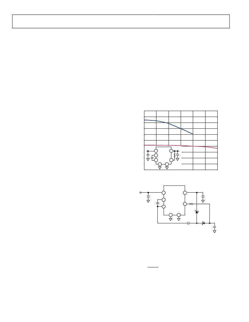
�–5�
�R� =� 29k?�
�feature� is� not� used,� Pin� 4� must� be� tied� to� the� ground� pin.�
�POWER� DISSIPATION�
�The� power� dissipation� of� the� ADP3605� circuit� must� be� limited�
�–4�
�V� IN� =� 5.0V�
�8�
�1�
�ADP3605�
�7�
�R�
�V� OUT�
�R� =� 24k?�
�such� that� the� junction� temperature� of� the� device� does� not� exceed�
�the� maximum� junction� temperature� rating.� Total� power� dissipation�
�3�
�4�
�2�
�5�
�is� calculated� as�
�P� =� (� V� IN� ?� |� V� OUT� |)� I� OUT� +� (� V� IN� )� I� S�
�–3�
�0�
�20�
�40� 60� 80�
�LOAD� CURRENT� (mA)�
�100�
�120�
�C� O�
�+� 4.7μF�
�1� C� P� +�
�1N5817�
�where:�
�I� OUT� and� I� S� are� output� current� and� supply� current,� respectively.�
�V� IN� and� V� OUT� are� input� and� output� voltages,� respectively.�
�For� example,� assuming� worst-case� conditions,� V� IN� =� 6� V,� V� OUT� =�
�?2.9� V,� I� OUT� =� 120� mA,� and� I� S� =� 5� mA.� Calculated� device� power�
�dissipation� is�
�P� ≈� (6� V� ?� |?2.9� V|)� 0.12� +� (6� V)� 0.005� A� =� 402� mW�
�V� IN� =� 5V�
�C� IN�
�4.7μF�
�Figure� 16.� Adjustable� Regulated� Output� Voltage�
�ADP3605�
�8� V� IN� V� OUT� 7�
�+�
�R1�
�C� P� +� 44.2k?�
�4.7μF� V� SENSE� 5�
�3� C� P� –�
�SD� GND� D1�
�4� 2�
�V� OUT� =�
�R�
�This� is� far� below� the� 660� mW� power� dissipation� capability� of�
��GENERAL� BOARD� LAYOUT� GUIDELINES�
�Because� the� internal� switches� of� the� ADP3605� turn� on� and� off�
�very� fast,� good� printed� circuit� board� (PCB)� layout� practices� are�
�critical� to� ensure� optimal� operation� of� the� device.� Improper� layouts�
�results� in� poor� load� regulation,� especially� under� heavy� loads.�
�Output� performance� can� be� improved� by� following� these�
�simple� layout� guidelines:�
�?� Use� adequate� ground� and� power� traces� or� planes�
�?� Use� single� point� ground� for� device� ground� and� input� and�
�output� capacitor� grounds�
�+�
�C1� D2� 10μF�
�4.7μF� 1N5817� +�
�Figure� 17.� Regulated� ?7� V� from� a� 5� V� Input�
�High� accuracy� on� the� adjustable� output� voltage� is� achieved� with�
�the� use� of� precision� trimmed� internal� resistors,� which� eliminate� the�
�need� to� trim� the� external� resistor� or� add� a� second� resistor� to� form� a�
�divider.� The� adjustable� output� voltage� is� set� by�
�1� .� 5�
�9� .� 5� k�
�where� V� OUT� is� in� volts� and� R� is� in� kΩ.�
�?�
�?�
�Keep� external� components� as� close� to� the� device� as� possible�
�Use� short� traces� from� the� input� and� output� capacitors� to�
�the� input� and� output� pins,� respectively�
�Rev.� B� |� Page� 10� of� 12�
�相关PDF资料 |
PDF描述 |
|---|---|
| ADP4000JCPZ-RL7 | IC PWR CTRL PMBUS 48-LFCSP |
| ADP4100JCPZ-RL7 | IC POWER CTLR VR11.1 48-LFCSP |
| ADP5020ACPZ-R7 | IC REG LDO DUAL BUCK 20LFCSP |
| ADP5065ACBZ-1-R7 | IC BATTERY MANAGEMENT 20WLCSP |
| ADP667ARZ-REEL7 | IC REG LDO 5V/ADJ .25A 8SOIC |
相关代理商/技术参数 |
参数描述 |
|---|---|
| ADP3605ARZ-3 | 制造商:Analog Devices 功能描述: |
| ADP3605ARZ-R7 | 功能描述:IC REG SWITCHD CAP INV ADJ 8SOIC RoHS:是 类别:集成电路 (IC) >> PMIC - 稳压器 - DC DC 开关稳压器 系列:- 产品培训模块:High Efficiency Current Mode Switching Regulators CMOS LDO Regulators 特色产品:BD91x Series Step-Down Regulators 标准包装:2,500 系列:- 类型:降压(降压) 输出类型:两者兼有 输出数:2 输出电压:3.3V,0.8 V ~ 2.5 V 输入电压:4.5 V ~ 5.5 V PWM 型:电流模式 频率 - 开关:1MHz 电流 - 输出:1.5A 同步整流器:是 工作温度:-40°C ~ 85°C 安装类型:表面贴装 封装/外壳:20-VFQFN 裸露焊盘 包装:带卷 (TR) 供应商设备封装:VQFN020V4040 产品目录页面:1373 (CN2011-ZH PDF) 其它名称:BD9152MUV-E2TR |
| ADP3607 | 制造商:AD 制造商全称:Analog Devices 功能描述:50 mA Switched Capacitor Voltage Boost with Regulated Output |
| ADP3607AR | 制造商:Analog Devices 功能描述:Charge Pump STPUP 3V to 9V 50mA 8-Pin SOIC 制造商:Rochester Electronics LLC 功能描述:SWTCHD CAPCTR VLT BOOST W/REGLTD OUTPUT - Bulk |
| ADP3607AR5 | 制造商:Analog Devices 功能描述: |
发布紧急采购,3分钟左右您将得到回复。