- 您现在的位置:买卖IC网 > PDF目录294846 > ADP3630ARZ-R7 (ANALOG DEVICES INC) High Speed, Dual, 2 A MOSFET Driver, non-inverting A/B input pins; Package: 8 ld SOIC; No of Pins: 8; Temperature Range: Ind PDF资料下载
参数资料
| 型号: | ADP3630ARZ-R7 |
| 厂商: | ANALOG DEVICES INC |
| 元件分类: | MOSFETs |
| 英文描述: | High Speed, Dual, 2 A MOSFET Driver, non-inverting A/B input pins; Package: 8 ld SOIC; No of Pins: 8; Temperature Range: Ind |
| 中文描述: | 2 A 2 CHANNEL, BUF OR INV BASED MOSFET DRIVER, PDSO8 |
| 封装: | ROHS COMPLIANT, MS-012-AA, SOIC-8 |
| 文件页数: | 4/16页 |
| 文件大小: | 361K |
| 代理商: | ADP3630ARZ-R7 |
ADP3629/ADP3630/ADP3631
Rev. 0 | Page 12 of 16
OVERTEMPERATURE PROTECTIONS
The ADP3629/ADP3630/ADP3631 provide two levels of over-
temperature protection:
Overtemperature warning (OTW)
Overtemperature shutdown
The overtemperature warning is an open-drain logic signal and
is active low. In normal operation, when no thermal warning is
present, the signal is high, whereas when the warning threshold
is crossed, the signal is pulled low.
ADP1043
3.3V
VDD
PGND
FLAGIN
VDD
OTW
ADP3629/ADP3630/ADP3631
08
40
1-
0
19
Figure 23. OTW Signaling Scheme Example
The OTW open-drain configuration allows the connection
of multiple devices to the same warning bus in a wire-OR’ed
configuration, as shown in
The overtemperature shutdown turns off the device to protect it
in the event that the die temperature exceeds the absolute maxi-
mum limit of 150°C (see Table 2).
SUPPLY CAPACITOR SELECTION
A local bypass capacitor for the supply input (VDD) of the
ADP3629/ADP3630/ADP3631 is recommended to reduce the
noise and to supply some of the peak currents that are drawn.
An improper decoupling can dramatically increase the rise times,
cause excessive resonance on the OUTA and OUTB pins, and, in
some extreme cases, even damage the device due to inductive
overvoltage on the VDD or OUTA/OUTB pins.
The minimum capacitance required is determined by the size of
the gate capacitances being driven, but as a general rule, a 4.7 μF,
low ESR capacitor should be used. Multilayer ceramic chip
(MLCC) capacitors provide the best combination of low ESR
and small size. To further reduce noise, use a smaller ceramic
capacitor (100 nF) with a better high frequency characteristic
in parallel with the main capacitor.
Place the ceramic capacitor as close as possible to the ADP3629/
ADP3630/ADP3631 device and minimize the length of the
traces going from the capacitor to the power pins of the device.
PCB LAYOUT CONSIDERATIONS
Use the following general guidelines when designing printed
circuit boards (PCBs) for the ADP3629/ADP3630/ADP3631:
Trace out the high current paths and use short, wide
(>40 mil) traces to make these connections.
Minimize trace inductance between the OUTA and OUTB
outputs and the MOSFET gates.
Connect the PGND pin as close as possible to the source of
the MOSFETs.
Place the VDD bypass capacitor as close as possible to the
VDD and PGND pins.
When possible, use vias to other layers to maximize thermal
conduction away from the IC.
Figure 24 shows an example of the typical layout based on the
preceding guidelines.
08
40
1-
0
27
Figure 24. External Component Placement Example
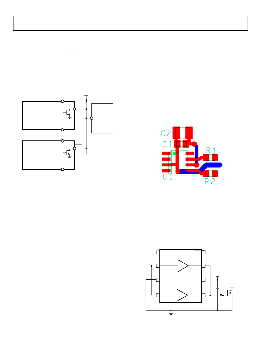
PARALLEL OPERATION
The two driver channels in the ADP3629 and ADP3630 devices
can be combined to operate in parallel to increase drive capability
and minimize power dissipation in the driver.
The connection scheme for the ADP3630 is shown in Figure 25.
In this configuration, INA and INB are connected together, and
OUTA and OUTB are connected together.
Particular attention must be paid to the layout in this case to
optimize load sharing between the two drivers.
INA
VDD
VDD
PGND
ADP3630
OUTA
OUTB
INB
SD
OTW
1
3
8
7
6
5
A
B
2
4
VDS
08
40
1-
02
1
Figure 25. Parallel Operation
相关PDF资料 |
PDF描述 |
|---|---|
| ADP3631ARMZ-R7 | High Speed, Dual, 2 A MOSFET Driver, inverting A & non-inverting B input pins; Package: 8 ld MSOP; No of Pins: 8; Temperature Range: Ind |
| ADP3631ARZ-R7 | High Speed, Dual, 2 A MOSFET Driver, inverting A & non-inverting B input pins; Package: 8 ld SOIC; No of Pins: 8; Temperature Range: Ind |
| ADP3820ART-4.2-RL | 1-CHANNEL POWER SUPPLY SUPPORT CKT, PDSO6 |
| ADPQ-ED12602/1 | 100 MHz - 160 MHz RF/MICROWAVE COMBINER |
| ADQ13Q006 | POWER/SIGNAL RELAY, SPST, LATCHED, 0.083A (COIL), 6VDC (COIL), 500mW (COIL), THROUGH HOLE-STRAIGHT MOUNT |
相关代理商/技术参数 |
参数描述 |
|---|---|
| ADP3630ARZ-R7 | 制造商:Analog Devices 功能描述:Dual Non-Inverting MOSFET Driver IC |
| ADP3631 | 制造商:AD 制造商全称:Analog Devices 功能描述:High Speed, Dual, 2 A MOSFET Driver |
| ADP3631ARMZ-R7 | 功能描述:IC MOSFET DVR 2A DL HS 8MSOP RoHS:是 类别:集成电路 (IC) >> PMIC - MOSFET,电桥驱动器 - 外部开关 系列:- 标准包装:50 系列:- 配置:低端 输入类型:非反相 延迟时间:40ns 电流 - 峰:9A 配置数:1 输出数:1 高端电压 - 最大(自引导启动):- 电源电压:4.5 V ~ 35 V 工作温度:-40°C ~ 125°C 安装类型:表面贴装 封装/外壳:TO-263-6,D²Pak(5 引线+接片),TO-263BA 供应商设备封装:TO-263 包装:管件 |
| ADP3631ARZ-R7 | 功能描述:IC MOSFET DVR 2A DL HS 8SOIC RoHS:是 类别:集成电路 (IC) >> PMIC - MOSFET,电桥驱动器 - 外部开关 系列:- 标准包装:95 系列:- 配置:高端和低端,独立 输入类型:非反相 延迟时间:160ns 电流 - 峰:290mA 配置数:1 输出数:2 高端电压 - 最大(自引导启动):600V 电源电压:10 V ~ 20 V 工作温度:-40°C ~ 125°C 安装类型:表面贴装 封装/外壳:8-SOIC(0.154",3.90mm 宽) 供应商设备封装:8-SOIC 包装:管件 产品目录页面:1381 (CN2011-ZH PDF) |
| ADP3633 | 制造商:AD 制造商全称:Analog Devices 功能描述:High Speed, Dual, 4 A MOSFET Driver with Thermal Protection |
发布紧急采购,3分钟左右您将得到回复。