- 您现在的位置:买卖IC网 > PDF目录11774 > ADP5585ACPZ-00-R7 (Analog Devices Inc)IC PORT EXPANDER 10I/O 16LFCSP PDF资料下载
参数资料
| 型号: | ADP5585ACPZ-00-R7 |
| 厂商: | Analog Devices Inc |
| 文件页数: | 4/40页 |
| 文件大小: | 0K |
| 描述: | IC PORT EXPANDER 10I/O 16LFCSP |
| 标准包装: | 1,500 |
| 系列: | * |
第1页第2页第3页当前第4页第5页第6页第7页第8页第9页第10页第11页第12页第13页第14页第15页第16页第17页第18页第19页第20页第21页第22页第23页第24页第25页第26页第27页第28页第29页第30页第31页第32页第33页第34页第35页第36页第37页第38页第39页第40页
ADP5585
Data Sheet
Rev. C | Page 12 of 40
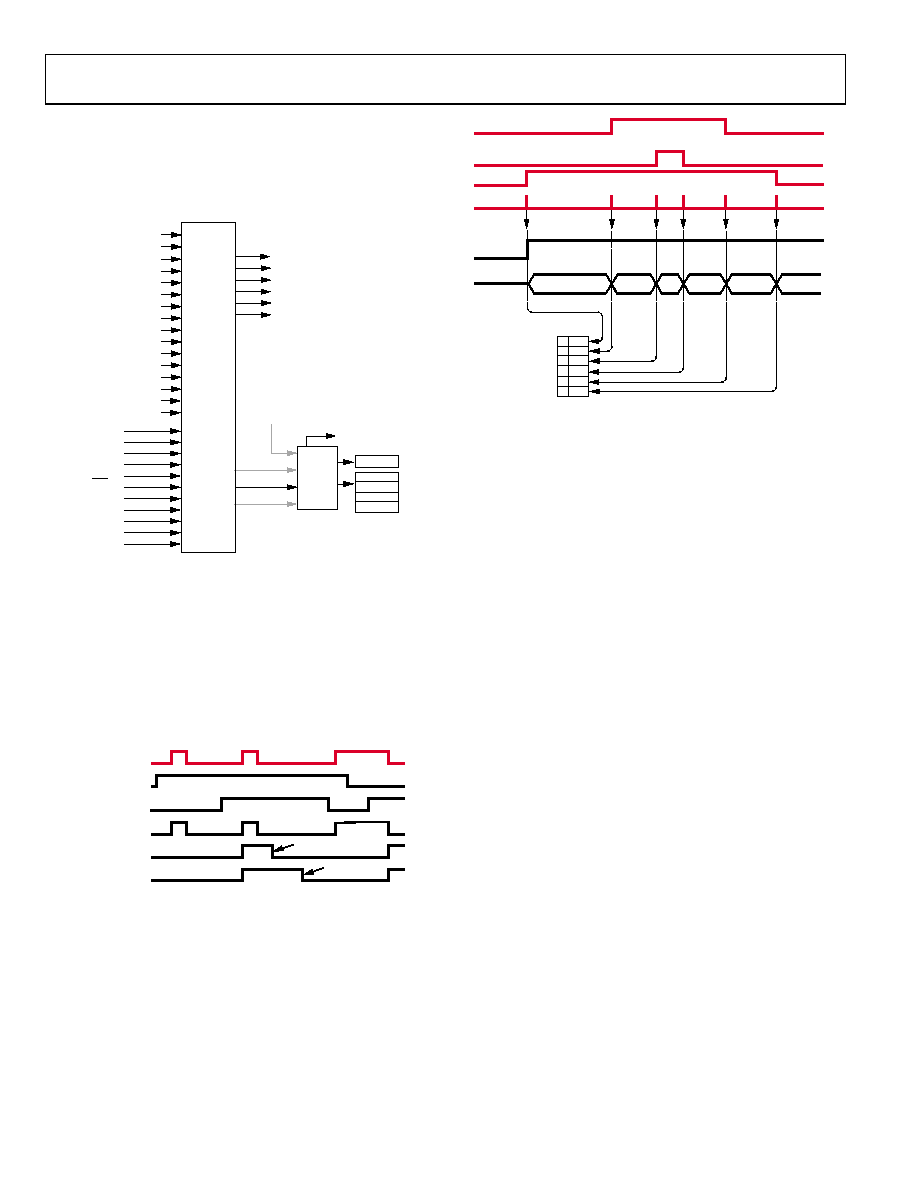
GPI INPUT
Each of the 10 input/output lines can be configured as a
general-purpose logic input line. Figure 15 shows a detailed
representation of the GPI scan and detect block and its
associated control and status signals.
PIN_CONFIG_A[7:0]
PIN_CONFIG_B[7:0]
GPI_INT
GPIO 1
GPIO 2
GPIO 3
GPIO 4
GPIO 5
GPIO 6
GPIO 7
GPIO 8
GPIO 9
(R0)
(R1)
(R2)
(R3)
(R4)
RST/(R5)
(C0)
(C1)
(C2)
GPIO 10
GPIO 11
(C3)
(C4)
GPI EVENT
KEY EVENT
OVRFLOW_INT
LOGIC EVENT
GPI_INT_LEVEL_A[7:0]
GPI_INT_LEVEL_B[7:0]
GPI_INTERRUPT_EN_A[7:0]
GPIO_DIRECTION_A[7:0]
GPI_STATUS_A[5:0]
GPI_STATUS_B[4:0]
GPI_INT_STAT_A[5:0]
GPI_EVENT_EN_A[7:0]
GPIO_DIRECTION_B[7:0]
GPI_INTERRUPT_EN_B[7:0]
GPI_EVENT_EN_B[7:0]
EVENT_INT
GPI_INT_STAT_B[4:0]
RESET_TRIG_TIME[2:0]
RESET1_EVENT_A[7:0]
RESET1_EVENT_B[7:0]
RESET1_EVENT_C[7:0]
RESET2_EVENT_A[7:0]
RESET2_EVENT_B[7:0]
FIFO1:FIFO16
EC[4:0]
09841-
014
FIFO
UPDATE
GPI SCAN
CONTROL
I2C BUSY
Figure 15. GPI Scan and Detect Block
The current input state of each GPI can be read back using the
GPI_STATUS_x registers. Each GPI can be programmed to
generate an interrupt via the GPI_INTERRUPT_EN_x registers.
The interrupt status is stored in the GPI_INT_STAT_x registers.
GPI interrupts can be programmed to trigger on the positive or
negative edge by configuring the GPI_INT_LEVEL_x registers.
If any of the GPI interrupts is triggered, the master GPI_INT
interrupt is also triggered. Figure 16 shows a single GPI and
how it affects its corresponding status and interrupt status bits.
GPI 3
GPI_STATUS_A[3]
GPI_INTERRUPT_EN_A[3]
GPI_INT_STAT_A[3]
GPI_INT
GPI_INT_LEVEL_A[3]
09841-
015
CLEARED
BY READ
CLEARED
BY WRITE ‘1’
Figure 16. Single GPI Example
GPIs can be programmed to generate FIFO events via the
GPI_EVENT_EN_x registers. GPIs in this mode do not generate
GPI_INT interrupts and instead generate EVENT_INT interrupts.
Figure 17 shows several GPI lines and their effects on the FIFO
and event count, EC[4:0].
GPI 2
GPI SCAN
EVENT_INT
EC[4:0]
1
6
GPI 2 ACTIVE
GPI 4
GPI 7
2
3
4
5
GPI 7 ACTIVE
GPI 4 ACTIVE
GPI 4 INACTIVE
GPI 7 INACTIVE
GPI 2 INACTIVE
FIFO
1
0
38
43
40
09841-
016
Figure 17. Multiple GPI Example
The GPI scanner is idle until it detects a level transition. It scans
the GPI inputs and updates accordingly. It then returns to idle
immediately, it does not scan/wait, like the key scanner. As
such, the GPI scanner can detect narrow pulses once they get
past the 50 μs input debounce filter.
GPO OUTPUT
Each of the 10 input/output lines can be configured as a general-
purpose output (GPO) line. Figure 6 shows a detailed diagram
of the I/O structure. See the Detailed Register Descriptions
section for GPO configuration and usage.
LOGIC BLOCKS
Several of the ADP5585 input/output lines can be used as inputs
and outputs for implementing some common logic functions.
The R1, R2, and R3 input/output pins can be used as inputs,
and the R0 input/output pin can be used as an output for the
logic block.
The outputs from the logic blocks can be configured to generate
interrupts. They can also be configured to generate events on
the FIFO.
Figure 19 shows a detailed diagram of the internal make-up of
the logic block, illustrating the possible logic functions that can
be implemented.
相关PDF资料 |
PDF描述 |
|---|---|
| PIC16LF1508-E/ML | IC MCU 8BIT 7KB FLASH 20-QFN |
| V110B36H150BG | CONVERTER MOD DC/DC 36V 150W |
| PIC16LF722A-I/MV | MCU PIC 3.5K FLASH XLP 28-UQFN |
| V110B36H150BF3 | CONVERTER MOD DC/DC 36V 150W |
| V110B36H150BF2 | CONVERTER MOD DC/DC 36V 150W |
相关代理商/技术参数 |
参数描述 |
|---|---|
| ADP5585ACPZ-01-R7 | 功能描述:IC PORT EXPANDER 10I/O 16LFCSP RoHS:是 类别:集成电路 (IC) >> 接口 - 专用 系列:* 特色产品:NXP - I2C Interface 标准包装:1 系列:- 应用:2 通道 I²C 多路复用器 接口:I²C,SM 总线 电源电压:2.3 V ~ 5.5 V 封装/外壳:16-TSSOP(0.173",4.40mm 宽) 供应商设备封装:16-TSSOP 包装:剪切带 (CT) 安装类型:表面贴装 产品目录页面:825 (CN2011-ZH PDF) 其它名称:568-1854-1 |
| ADP5585ACPZ-03-R7 | 功能描述:IC PORT EXPANDER 10I/O 16LFCSP RoHS:是 类别:集成电路 (IC) >> 接口 - 专用 系列:* 特色产品:NXP - I2C Interface 标准包装:1 系列:- 应用:2 通道 I²C 多路复用器 接口:I²C,SM 总线 电源电压:2.3 V ~ 5.5 V 封装/外壳:16-TSSOP(0.173",4.40mm 宽) 供应商设备封装:16-TSSOP 包装:剪切带 (CT) 安装类型:表面贴装 产品目录页面:825 (CN2011-ZH PDF) 其它名称:568-1854-1 |
| ADP5585CP-EVALZ | 功能描述:BOARD EVAL FOR ADP5585CP RoHS:是 类别:编程器,开发系统 >> 评估演示板和套件 系列:- 标准包装:1 系列:- 主要目的:电信,线路接口单元(LIU) 嵌入式:- 已用 IC / 零件:IDT82V2081 主要属性:T1/J1/E1 LIU 次要属性:- 已供物品:板,电源,线缆,CD 其它名称:82EBV2081 |
| ADP5586 | 制造商:AD 制造商全称:Analog Devices 功能描述:Keypad Decoder and I/O Port Expander |
| ADP5586ACBZ-00-R7 | 功能描述:接口-I/O扩展器 RoHS:否 制造商:NXP Semiconductors 逻辑系列: 输入/输出端数量: 最大工作频率:100 kHz 工作电源电压:1.65 V to 5.5 V 工作温度范围:- 40 C to + 85 C 安装风格:SMD/SMT 封装 / 箱体:HVQFN-16 封装:Reel |
发布紧急采购,3分钟左右您将得到回复。