- 您现在的位置:买卖IC网 > PDF目录11774 > ADP5585ACPZ-03-R7 (Analog Devices Inc)IC PORT EXPANDER 10I/O 16LFCSP PDF资料下载
参数资料
| 型号: | ADP5585ACPZ-03-R7 |
| 厂商: | Analog Devices Inc |
| 文件页数: | 7/40页 |
| 文件大小: | 0K |
| 描述: | IC PORT EXPANDER 10I/O 16LFCSP |
| 标准包装: | 1,500 |
| 系列: | * |
第1页第2页第3页第4页第5页第6页当前第7页第8页第9页第10页第11页第12页第13页第14页第15页第16页第17页第18页第19页第20页第21页第22页第23页第24页第25页第26页第27页第28页第29页第30页第31页第32页第33页第34页第35页第36页第37页第38页第39页第40页
Data Sheet
ADP5585
Rev. C | Page 15 of 40
REGISTER INTERFACE
Register access to the ADP5585 is acquired via its I2C-compatible
serial interface. The interface can support clock frequencies of
up to 1 MHz. If the user is accessing the FIFO or key event
counter (KEC), FIFO/KEC updates are paused. If the clock
frequency is very low, events may not be recorded in a timely
manner. FIFO or KEC updates can happen up to 23 μs after an
interrupt is asserted because of the number of I2C cycles required
to perform an I2C read or write. This delay should not present
an issue to the user.
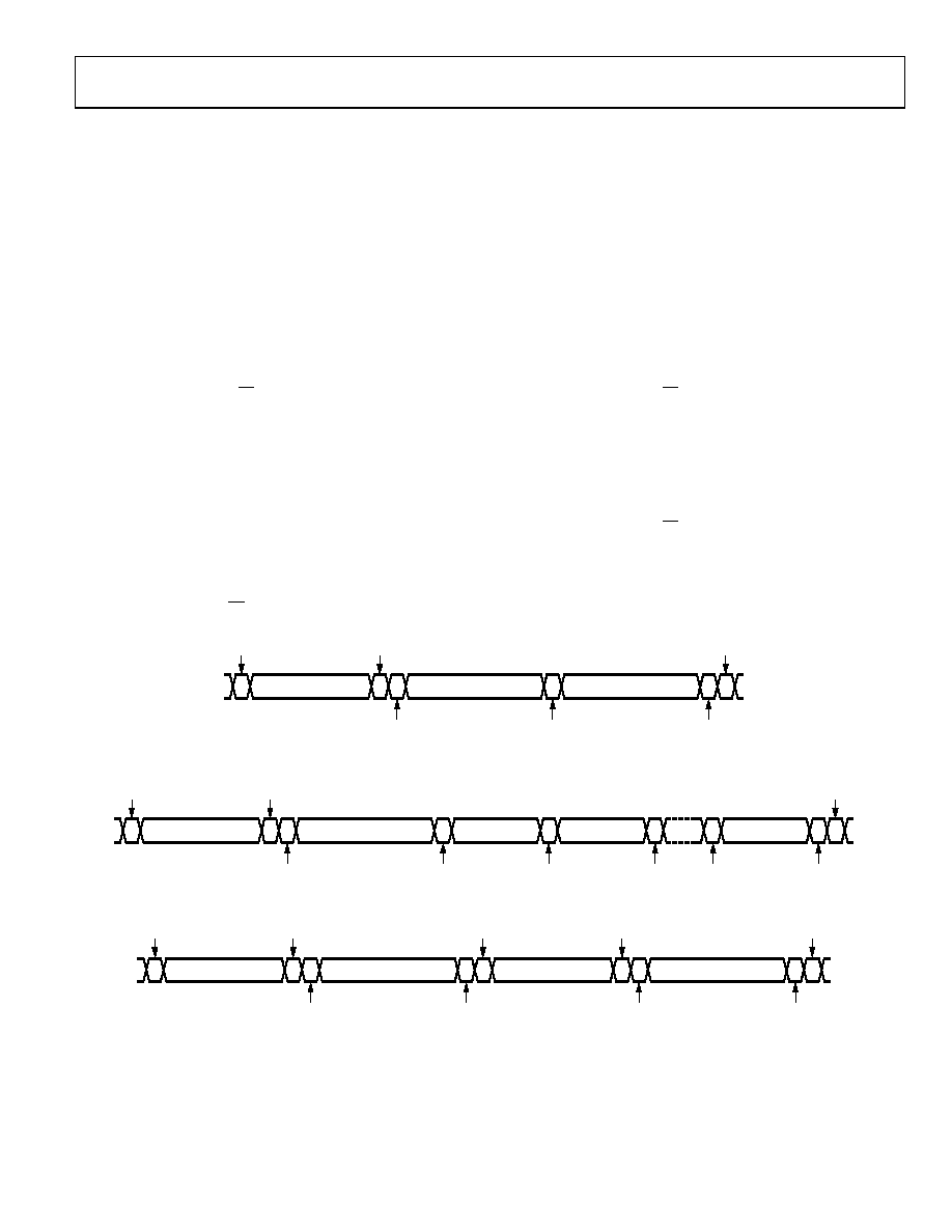
Figure 23 shows a typical write sequence for programming an
internal register. The cycle begins with a start condition, followed
by the hard coded 7-bit device address, which for the ADP5585
is 0x34, followed by the R/W bit set to 0 for a write cycle. The
ADP5585 acknowledges the address byte by pulling the data
line low. The address of the register to which data is to be written
is sent next. The ADP5585 acknowledges the register pointer
byte by pulling the data line low. The data byte to be written is
sent next. The ADP5585 acknowledges the data byte by pulling
the data line low. A stop condition completes the sequence.
Figure 24 shows a typical multibyte write sequence for program-
ming internal registers. The cycle begins with a start condition
followed by the 7-bit device address (0x34 for all models except
the ADP5585ACPZ-03-R7, 0x30 for the ADP5585ACPZ-03-R7
only), followed by the R/W bit set to 0 for a write cycle. The
ADP5585 acknowledges the address byte by pulling the data
line low. The address of the register to which data is to be written
is sent next. The ADP5585 acknowledges the register pointer
byte by pulling the data line low. The data byte to be written is
sent next. The ADP5585 acknowledges the data byte by pulling
the data line low. The pointer address is then incremented to
write the next data byte, until it finishes writing the n data byte.
The ADP5585 pulls the data line low after every byte, and a stop
condition completes the sequence.
Figure 25 shows a typical byte read sequence for reading inter-
nal registers. The cycle begins with a start condition followed
by the 7-bit device address (0x34 for all models except the
ADP5585ACPZ-03-R7, 0x30 for the ADP5585ACPZ-03-R7
only), followed by the R/W bit set to 0 for a write cycle. The
ADP5585 acknowledges the address byte by pulling the data line
low. The address of the register from which data is to be read is
sent next. The ADP5585 acknowledges the register pointer byte
by pulling the data line low. A start condition is repeated,
followed by the 7-bit device address (0x34 for all models except
the ADP5585ACPZ-03-R7, 0x30 for the ADP5585ACPZ-03-R7
only), followed by the R/W bit set to 1 for a read cycle. The
ADP5585 acknowledges the address byte by pulling the data
line low. The 8-bit data is then read. The host pulls the data line
high (no acknowledge), and a stop condition completes the
sequence.
START
0 = WRITE
7-BIT DEVICE ADDRESS
ADP5585 ACK
8-BIT REGISTER POINTER
8-BIT WRITE DATA
0
000
ADP5585 ACK
STOP
09
84
1-
02
2
Figure 23. I2C Single Byte Write Sequence
START
0 = WRITE
7-BIT DEVICE ADDRESS
ADP5585 ACK
8-BIT REGISTER POINTER
WRITE BYTE 1
WRITE BYTE 2
WRITE BYTE n
00
0
ADP5585 ACK
STOP
09
84
1-
02
3
Figure 24. I2C Multibyte Write Sequence
START
0 = WRITE
7-BIT DEVICE ADDRESS
ADP5585 ACK
8-BIT REGISTER POINTER
8-BIT READ DATA
00
0
1
0
1
REPEAT START
1 = READ
ADP5585 ACK
NO ACK
STOP
09
84
1-
02
4
Figure 25. I2C Single Byte Read Sequence
相关PDF资料 |
PDF描述 |
|---|---|
| V110B36H150BG3 | CONVERTER MOD DC/DC 36V 150W |
| ADP5585ACPZ-00-R7 | IC PORT EXPANDER 10I/O 16LFCSP |
| PIC16LF1508-E/ML | IC MCU 8BIT 7KB FLASH 20-QFN |
| V110B36H150BG | CONVERTER MOD DC/DC 36V 150W |
| PIC16LF722A-I/MV | MCU PIC 3.5K FLASH XLP 28-UQFN |
相关代理商/技术参数 |
参数描述 |
|---|---|
| ADP5585CP-EVALZ | 功能描述:BOARD EVAL FOR ADP5585CP RoHS:是 类别:编程器,开发系统 >> 评估演示板和套件 系列:- 标准包装:1 系列:- 主要目的:电信,线路接口单元(LIU) 嵌入式:- 已用 IC / 零件:IDT82V2081 主要属性:T1/J1/E1 LIU 次要属性:- 已供物品:板,电源,线缆,CD 其它名称:82EBV2081 |
| ADP5586 | 制造商:AD 制造商全称:Analog Devices 功能描述:Keypad Decoder and I/O Port Expander |
| ADP5586ACBZ-00-R7 | 功能描述:接口-I/O扩展器 RoHS:否 制造商:NXP Semiconductors 逻辑系列: 输入/输出端数量: 最大工作频率:100 kHz 工作电源电压:1.65 V to 5.5 V 工作温度范围:- 40 C to + 85 C 安装风格:SMD/SMT 封装 / 箱体:HVQFN-16 封装:Reel |
| ADP5586ACBZ-01-R7 | 功能描述:接口-I/O扩展器 RoHS:否 制造商:NXP Semiconductors 逻辑系列: 输入/输出端数量: 最大工作频率:100 kHz 工作电源电压:1.65 V to 5.5 V 工作温度范围:- 40 C to + 85 C 安装风格:SMD/SMT 封装 / 箱体:HVQFN-16 封装:Reel |
| ADP5586ACBZ-03-R7 | 功能描述:接口-I/O扩展器 RoHS:否 制造商:NXP Semiconductors 逻辑系列: 输入/输出端数量: 最大工作频率:100 kHz 工作电源电压:1.65 V to 5.5 V 工作温度范围:- 40 C to + 85 C 安装风格:SMD/SMT 封装 / 箱体:HVQFN-16 封装:Reel |
发布紧急采购,3分钟左右您将得到回复。