- 您现在的位置:买卖IC网 > PDF目录11774 > ADP5589ACBZ-01-R7 (Analog Devices Inc)IC PORT EXPANDER 19I/O 25WLSCP PDF资料下载
参数资料
| 型号: | ADP5589ACBZ-01-R7 |
| 厂商: | Analog Devices Inc |
| 文件页数: | 11/52页 |
| 文件大小: | 0K |
| 描述: | IC PORT EXPANDER 19I/O 25WLSCP |
| 产品变化通告: | 8mm Carrier Tape Changes 28/Feb/2012 |
| 标准包装: | 3,000 |
| 系列: | * |
第1页第2页第3页第4页第5页第6页第7页第8页第9页第10页当前第11页第12页第13页第14页第15页第16页第17页第18页第19页第20页第21页第22页第23页第24页第25页第26页第27页第28页第29页第30页第31页第32页第33页第34页第35页第36页第37页第38页第39页第40页第41页第42页第43页第44页第45页第46页第47页第48页第49页第50页第51页第52页
Data Sheet
ADP5589
Rev. B | Page 19 of 52
REGISTER INTERFACE
serial interface. The interface can support clock frequencies of
up to 1 MHz. If the user is accessing the FIFO or key event
counter (KEC), FIFO/KEC updates are paused. If the clock
frequency is very low, events may not be recorded in a timely
manner. FIFO or KEC updates can happen up to 23 μs after an
interrupt is asserted because of the number of I2C cycles required
to perform an I2C read or write. This delay should not present
an issue to the user.
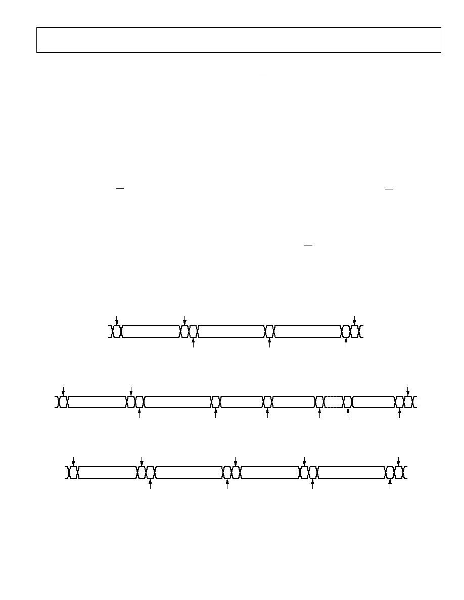
Figure 27 shows a typical write sequence for programming an
internal register. The cycle begins with a start condition, followed
by the hard coded 7-bit device address, which for the ADP5589
is 0x34, followed by the R/W bit set to 0 for a write cycle. The
ADP5589 acknowledges the address byte by pulling the data line
low. The address of the register to which data is to be written is
sent next. The ADP5589 acknowledges the register pointer byte
by pulling the data line low. The data byte to be written is sent
next. The ADP5589 acknowledges the data byte by pulling the
data line low. A stop condition completes the sequence.
Figure 28 shows a typical multibyte write sequence for program-
ming internal registers. The cycle begins with a start condition
followed by the 7-bit device address (0x34), followed by the
R/W bit set to 0 for a write cycle. The ADP5589 acknowledges
the address byte by pulling the data line low. The address of the
register to which data is to be written is sent next. The ADP5589
acknowledges the register pointer byte by pulling the data line
low. The data byte to be written is sent next. The ADP5589
acknowledges the data byte by pulling the data line low. The
pointer address is then incremented to write the next data byte,
until it finishes writing the n data byte. The ADP5589 pulls the
data line low after every byte, and a stop condition completes
the sequence.
Figure 29 shows a typical byte read sequence for reading internal
registers. The cycle begins with a start condition followed by the
7-bit device address (0x34), followed by the R/W bit set to 0 for
a write cycle. The ADP5589 acknowledges the address byte by
pulling the data line low. The address of the register from which
data is to be read is sent next. The ADP5589 acknowledges the
register pointer byte by pulling the data line low. A start condi-
tion is repeated, followed by the 7-bit device address (0x34),
followed by the R/W bit set to 1 for a read cycle. The ADP5589
acknowledges the address byte by pulling the data line low. The
8-bit data is then read. The host pulls the data line high (no
acknowledge), and a stop condition completes the sequence.
START
0 = WRITE
7-BIT DEVICE ADDRESS
ADP5589 ACK
8-BIT REGISTER POINTER
8-BIT WRITE DATA
00
0
ADP5589 ACK
STOP
097
14-
02
6
Figure 27. I2C Single-Byte Write Sequence
START
0 = WRITE
7-BIT DEVICE ADDRESS
ADP5589 ACK
8-BIT REGISTER POINTER
WRITE BYTE 1
WRITE BYTE 2
WRITE BYTE n
00
0
ADP5589 ACK
STOP
0971
4-
028
Figure 28. I2C Multibyte Write Sequence
START
0 = WRITE
7-BIT DEVICE ADDRESS
ADP5589 ACK
8-BIT REGISTER POINTER
8-BIT READ DATA
00
0
1
0
1
REPEAT START
1 = READ
ADP5589 ACK
NO ACK
STOP
0971
4-
027
Figure 29. I2C Single-Byte Read Sequence
相关PDF资料 |
PDF描述 |
|---|---|
| PIC12F675-I/MF | IC MCU CMOS 1K FLASH W/AD 8-DFN |
| V150B3V3H100B2 | CONVERTER MOD DC/DC 3.3V 100W |
| V150B3V3H100B | CONVERTER MOD DC/DC 3.3V 100W |
| PIC16F1508-E/ML | IC MCU 8BIT 7KB FLASH 20-QFN |
| ADP5585ACPZ-03-R7 | IC PORT EXPANDER 10I/O 16LFCSP |
相关代理商/技术参数 |
参数描述 |
|---|---|
| ADP5589ACBZ-02-R7 | 功能描述:IC PORT EXPANDER 19I/O 25WLSCP RoHS:是 类别:集成电路 (IC) >> 接口 - 专用 系列:* 特色产品:NXP - I2C Interface 标准包装:1 系列:- 应用:2 通道 I²C 多路复用器 接口:I²C,SM 总线 电源电压:2.3 V ~ 5.5 V 封装/外壳:16-TSSOP(0.173",4.40mm 宽) 供应商设备封装:16-TSSOP 包装:剪切带 (CT) 安装类型:表面贴装 产品目录页面:825 (CN2011-ZH PDF) 其它名称:568-1854-1 |
| ADP5589ACPZ | 制造商:Analog Devices 功能描述:I/O EXPANDER 19IO KEY DECODER 24LFCSP 制造商:Analog Devices 功能描述:I/O EXPANDER, 19IO, KEY DECODER, 24LFCSP 制造商:Analog Devices 功能描述:I/O EXPANDER, 19IO, KEY DECODER, 24LFCSP, Chip Configuration:8bit, IC Interface 制造商:Analog Devices 功能描述:I/O EXPANDER, 19IO, KEY DECODER, 24LFCSP, Chip Configuration:8bit, IC Interface Type:I2C, Supply Voltage Min:1.65V, Supply Voltage Max:3.6V, Digital IC Case Style:LFCSP, No. of Pins:24, No. of I/O's:19, MSL:MSL 3 - 168 hours, SVHC:No |
| ADP5589ACPZ-00-R7 | 功能描述:IC KEY DECODER 19I/O EXP 24LFCSP RoHS:是 类别:集成电路 (IC) >> 接口 - 专用 系列:- 特色产品:NXP - I2C Interface 标准包装:1 系列:- 应用:2 通道 I²C 多路复用器 接口:I²C,SM 总线 电源电压:2.3 V ~ 5.5 V 封装/外壳:16-TSSOP(0.173",4.40mm 宽) 供应商设备封装:16-TSSOP 包装:剪切带 (CT) 安装类型:表面贴装 产品目录页面:825 (CN2011-ZH PDF) 其它名称:568-1854-1 |
| ADP5589ACPZ-01-R7 | 功能描述:IC KEY DECODER 19I/O EXP 24LFCSP RoHS:是 类别:集成电路 (IC) >> 接口 - 专用 系列:- 特色产品:NXP - I2C Interface 标准包装:1 系列:- 应用:2 通道 I²C 多路复用器 接口:I²C,SM 总线 电源电压:2.3 V ~ 5.5 V 封装/外壳:16-TSSOP(0.173",4.40mm 宽) 供应商设备封装:16-TSSOP 包装:剪切带 (CT) 安装类型:表面贴装 产品目录页面:825 (CN2011-ZH PDF) 其它名称:568-1854-1 |
| ADP5589ACPZ-02-R7 | 功能描述:IC KEY DECODER 19I/O EXP 24LFCSP RoHS:是 类别:集成电路 (IC) >> 接口 - 专用 系列:- 特色产品:NXP - I2C Interface 标准包装:1 系列:- 应用:2 通道 I²C 多路复用器 接口:I²C,SM 总线 电源电压:2.3 V ~ 5.5 V 封装/外壳:16-TSSOP(0.173",4.40mm 宽) 供应商设备封装:16-TSSOP 包装:剪切带 (CT) 安装类型:表面贴装 产品目录页面:825 (CN2011-ZH PDF) 其它名称:568-1854-1 |
发布紧急采购,3分钟左右您将得到回复。