- 您现在的位置:买卖IC网 > PDF目录375262 > ADR127BUJZ-REEL7 (ANALOG DEVICES INC) Precision, Micropower LDO Voltage References in TSOT PDF资料下载
参数资料
| 型号: | ADR127BUJZ-REEL7 |
| 厂商: | ANALOG DEVICES INC |
| 元件分类: | 基准电压源/电流源 |
| 英文描述: | Precision, Micropower LDO Voltage References in TSOT |
| 中文描述: | 1-OUTPUT THREE TERM VOLTAGE REFERENCE, 1.25 V, PDSO6 |
| 封装: | ROHS COMPLIANT, MO-193AA, TSOT-6 |
| 文件页数: | 17/20页 |
| 文件大小: | 484K |
| 代理商: | ADR127BUJZ-REEL7 |
ADR121/ADR125/ADR127
APPLICATIONS
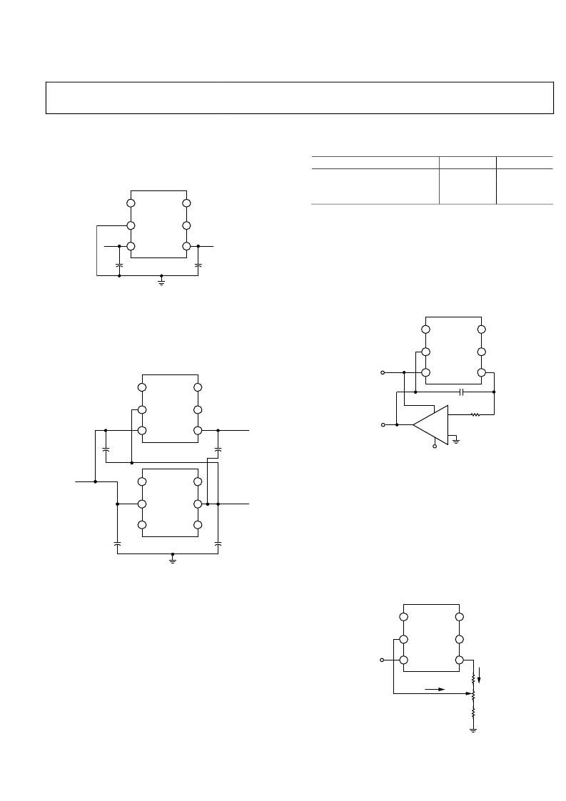
BASIC VOLTAGE REFERENCE CONNECTION
The circuit in Figure 4 illustrates the basic configuration for the
ADR12x family voltage reference.
Rev. 0 | Page 17 of 20
NC
V
OUT
NC
ADR12x
1
2
3
6
5
4
NC
GND
V
IN
0.1μF
0.1μF
OUTPUT
INPUT
+
+
0
Figure 49. Basic Configuration for the ADR12x Family
STACKING REFERENCE ICs FOR ARBITRARY
OUTPUTS
Some applications may require two reference voltage sources
that are a combined sum of the standard outputs. Figure 50
shows how this stacked output reference can be implemented.
NC
V
OUT
NC
ADR12x
1
2
3
6
5
4
NC
GND
V
IN
0.1μF
0.1μF
OUTPUT1
+
+
NC
V
OUT
NC
ADR12x
1
2
3
6
5
4
NC
GND
V
IN
0.1μF
0.1μF
OUTPUT2
INPUT
+
+
0
Figure 50. Stacking References with ADR12x
Two reference ICs are used and fed from an unregulated input,
V
IN
. The outputs of the individual ICs are connected in series,
which provide two output voltages, V
OUT1
and V
OUT2
. V
OUT1
is the
terminal voltage of U1, while V
OUT2
is the sum of this voltage
and the terminal of U2. U1 and U2 are chosen for the two
voltages that supply the required outputs (see Table 6). For
example, if U1 and U2 are ADR127 and V
IN
≥ 3.95 V, V
OUT1
is
1.25 V and V
OUT2
is 2.5 V.
Table 6. Required Outputs
U1/U2
ADR127/ADR121
ADR127/ADR125
ADR121/ADR125
V
OUT2
1.25 V
1.25 V
2.5 V
V
OUT1
3.75 V
6.25 V
7.5 V
NEGATIVE PRECISION REFERENCE WITHOUT
PRECISION RESISTORS
A negative reference is easily generated by adding an op amp,
A1, and is configured as shown in Figure 51. V
OUT1
is at virtual
ground and, therefore, the negative reference can be taken
directly from the output of the op amp. The op amp must be
dual-supply, low offset, and rail-to-rail if the negative supply
voltage is close to the reference output.
NC
V
OUT
NC
ADR127
AD8603
V–
1
2
3
6
5
4
NC
GND
–
V+
3
2
+
V
IN
0
0.1μF
+V
DD
–V
REF
1k
–V
DD
Figure 51. Negative Reference
GENERAL-PURPOSE CURRENT SOURCE
In low power applications, the need can arise for a precision
current source that can operate on low supply voltages. The
ADR12x can be configured as a precision current source (see
Figure 52). The circuit configuration shown is a floating current
source with a grounded load. The reference’s output voltage is
bootstrapped across R
SET
, which sets the output current into the
load. With this configuration, circuit precision is maintained for
load currents ranging from the reference’s supply current,
typically 85 μA, to approximately 5 mA.
NC
V
OUT
NC
R1
ADR12x
1
2
3
6
5
4
NC
GND
V
IN
I
SY
+V
DD
RL
P1
I
SET
0
Figure 52. ADR12x Trim Configuration
相关PDF资料 |
PDF描述 |
|---|---|
| ADR130 | Precision Series Sub-Band Gap Voltage Reference |
| ADR130AUJZ-R2 | Precision Series Sub-Band Gap Voltage Reference |
| ADR130AUJZ-REEL7 | Precision Series Sub-Band Gap Voltage Reference |
| ADR130BUJZ-R2 | Precision Series Sub-Band Gap Voltage Reference |
| ADR130BUJZ-REEL7 | Precision Series Sub-Band Gap Voltage Reference |
相关代理商/技术参数 |
参数描述 |
|---|---|
| ADR127BUJZ-REEL71 | 制造商:AD 制造商全称:Analog Devices 功能描述:Precision, Micropower LDO Voltage References in TSOT |
| ADR130 | 制造商:AD 制造商全称:Analog Devices 功能描述:Precision Series Sub-Band Gap Voltage Reference |
| ADR130AUJZ-R2 | 功能描述:IC VREF SERIES PREC 0.5V TSOT-6 RoHS:是 类别:集成电路 (IC) >> PMIC - 电压基准 系列:- 产品培训模块:Voltage Reference Basics 标准包装:100 系列:- 基准类型:旁路,精度 输出电压:4.096V 容差:±0.075% 温度系数:50ppm/°C 输入电压:- 通道数:1 电流 - 阴极:1µA 电流 - 静态:- 电流 - 输出:10mA 工作温度:0°C ~ 70°C 安装类型:表面贴装 封装/外壳:8-SOIC(0.154",3.90mm 宽) 供应商设备封装:8-SOIC 包装:管件 |
| ADR130AUJZ-REEL7 | 功能描述:IC VREF SERIES PREC 0.5V TSOT-6 RoHS:是 类别:集成电路 (IC) >> PMIC - 电压基准 系列:- 标准包装:3,000 系列:- 基准类型:旁路,精度 输出电压:3V 容差:±0.5% 温度系数:100ppm/°C 输入电压:- 通道数:1 电流 - 阴极:82µA 电流 - 静态:- 电流 - 输出:15mA 工作温度:-40°C ~ 85°C 安装类型:表面贴装 封装/外壳:6-TSSOP(5 引线),SC-88A,SOT-353 供应商设备封装:SC-70-5 包装:带卷 (TR) 其它名称:296-20888-2 |
| ADR130BUJZ | 制造商:Analog Devices 功能描述:IC SM VOLT REF 0.5/1V 制造商:Analog Devices 功能描述:IC, SM, VOLT REF, 0.5/1V |
发布紧急采购,3分钟左右您将得到回复。