- 您现在的位置:买卖IC网 > PDF目录1778 > ADR280AKS-R2 (Analog Devices Inc)IC VREF SERIES PREC 1.2V SC-70-3 PDF资料下载
参数资料
| 型号: | ADR280AKS-R2 |
| 厂商: | Analog Devices Inc |
| 文件页数: | 9/12页 |
| 文件大小: | 0K |
| 描述: | IC VREF SERIES PREC 1.2V SC-70-3 |
| 设计资源: | 4 mA-to-20 mA Loop-Powered Temperature Monitor Using ADuC7060/1 (CN0145) |
| 标准包装: | 1 |
| 基准类型: | 串联,精度 |
| 输出电压: | 1.2V |
| 容差: | ±0.4% |
| 温度系数: | 40ppm/°C |
| 输入电压: | 2.4 V ~ 5.5 V |
| 通道数: | 1 |
| 电流 - 静态: | 16µA |
| 电流 - 输出: | 100µA |
| 工作温度: | -40°C ~ 85°C |
| 安装类型: | 表面贴装 |
| 封装/外壳: | SC-70,SOT-323 |
| 供应商设备封装: | SC-70-3 |
| 包装: | 剪切带 (CT) |
| 其它名称: | ADR280AKS-R2CT |
�� �
�
�ADR280�
�Boosted� Current� Source�
�Adding� one� more� buffer� to� the� previous� circuit� boosts� the�
�current� to� the� level� that� is� limited� only� by� the� buffer� U2� current�
�handling� capability� (see� Figure� 18).�
�U1�
�100� mA� load� is� achievable� at� a� 5� V� supply.� The� higher� the�
�supply� voltage,� the� lower� the� current� handling� is� because� of� the�
�heat� generated� on� the� MOSFET.� For� heavy� capacitive� loads,�
�additional� buffering� is� needed� at� the� output� to� enhance� the�
�transient� response.�
�5V�
�5V�
�V+�
�ADR280�
�V–�
�2.5V/100mA�
�V� O�
�RL�
�25� ?�
�M1*�
�5V�
�U1�
�V+�
�ADR280�
�V–�
�U2�
�V+�
�V–�
�V� OUT�
�C1�
�0.1μF�
�R2�
�10.8k� ?� ±� 0.1%�
�C2�
�1pF�
�U2�
�+�
�V+�
�AD8541�
�V–� –�
�V� REF�
�1.2V�
�V� OUT�
�C1�
�0.1μF�
�+�
�R� SET�
�230� ?�
�RL�
�500� ?�
�+�
�1.2V�
�–�
�I� L�
�5mA�
�5V�
�–� U3�
�V+�
�V–�
�I� L� =� 1.2V/R� SET�
�U2� =� U3� =� AD8542,� AD822�
�R1� *M1� =� FDB301N,� 2N7000,� 2N7002,� OR� EQUIVALENT.�
�10k� ?� ±� 0.1%�
�Figure� 20.� 2.5� V� Boosted� Reference�
�GSM� and� 3G� Mobile� Station� Applications�
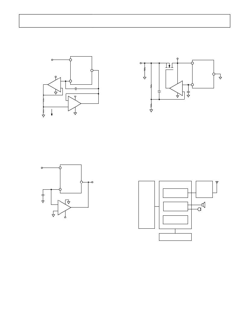
�Figure� 18.� Precision� Current� Source�
�Negative� Reference�
�A� negative� reference� can� be� precisely� configured� without� using�
��The� voltage� difference� between� V� OUT� and� V?� is� 1.2� V.� Since� V� OUT�
�is� at� virtual� ground,� U2� closes� the� loop� by� forcing� the� V?� pin� to�
�be� the� negative� reference� output.�
�U1�
�The� ADR280� voltage� reference� is� ideal� for� use� with� analog�
�baseband� ICs� in� GSM� and� 3G� mobile� station� applications.�
��GSM� analog� baseband.� The� AD6535� provides� all� of� the� data�
�converters� and� power� management� functions� needed� to�
�implement� a� GSM� mobile� station,� including� baseband� codecs,�
�audio� codecs,� voltage� regulators,� and� a� battery� charger.� Besides�
�low� current� consumption� and� a� small� footprint,� the� ADR280� is�
�+5V�
�V+�
�ADR280�
�optimized� for� excellent� PSRR,� which� is� necessary� for� optimum�
�AD6535� device� performance� when� the� main� battery� voltage�
�fluctuates� during� RF� power� amplifier� activity.�
�V–�
�–V� REF�
�–1.2V�
�DIGITAL�
�BASEBAND�
�AD6535�
�ANALOG� BASEBAND�
�RADIO�
�V� OUT�
�C1�
�0.1μF�
�U2�
�BASEBAND� CODEC�
�V+�
�–�
�AD8541�
�AUDIO� CODEC�
�+�
�V–�
�–2.7V�
�Figure� 19.� Negative� Reference�
�Boosted� Reference� with� Scalable� Output�
�A� precision� user� defined� output� with� boosted� current� capability�
�can� be� implemented� with� the� circuit� shown� in� Figure� 20.� In� this�
�circuit,� U2� forces� V� O� to� be� equal� to� V� REF� � (1� +� R2/R1)� by� regu-�
�lating� the� turn-on� of� M1;� the� load� current� is� therefore� furnished�
�by� the� 5� V� supply.� For� higher� output� voltage,� U2� must� be� changed�
�and� the� supply� voltage� of� M1� and� U2� must� also� be� elevated� and�
�separated� from� the� U1� input� voltage.� In� this� configuration,� a�
�Rev.� C� |� Page� 9� of� 12�
�POWER�
�MANAGEMENT�
�ADR280�
�VOLTAGE� REFERENCE�
�Figure� 21.� GSM� Mobile� Station� Application�
�相关PDF资料 |
PDF描述 |
|---|---|
| ADR292FRZ-REEL | IC VREF SERIES PREC 4.096V 8SOIC |
| ADR293ERZ-REEL | IC VREF SERIES PREC 5V 8-SOIC |
| ADR318ARJ-R2 | IC VREF SERIES PREC 1.8V SOT23-5 |
| ADR370BRT-R2 | IC VREF SERIES PREC SOT-23-3 |
| ADR390BUJZ-REEL7 | IC VREF SERIES PREC TSOT-23-5 |
相关代理商/技术参数 |
参数描述 |
|---|---|
| ADR280AKS-REEL | 制造商:Analog Devices 功能描述: |
| ADR280AKS-REEL7 | 制造商:Analog Devices 功能描述:V-Ref Precision 1.2V 100mA 3-Pin SC-70 T/R |
| ADR280AKSZ-R2 | 功能描述:IC VREF SERIES PREC 1.2V SC-70-3 RoHS:是 类别:集成电路 (IC) >> PMIC - 电压基准 系列:- 产品培训模块:Voltage Reference Basics 标准包装:100 系列:- 基准类型:旁路,精度 输出电压:4.096V 容差:±0.075% 温度系数:50ppm/°C 输入电压:- 通道数:1 电流 - 阴极:1µA 电流 - 静态:- 电流 - 输出:10mA 工作温度:0°C ~ 70°C 安装类型:表面贴装 封装/外壳:8-SOIC(0.154",3.90mm 宽) 供应商设备封装:8-SOIC 包装:管件 |
| ADR280AKSZ-R21 | 制造商:AD 制造商全称:Analog Devices 功能描述:1.2 V Ultralow Power High PSRR Voltage Reference |
| ADR280AKSZ-REEL7 | 功能描述:IC VREF SERIES PREC 1.2V SC-70-3 RoHS:是 类别:集成电路 (IC) >> PMIC - 电压基准 系列:- 标准包装:3,000 系列:- 基准类型:旁路,精度 输出电压:3V 容差:±0.5% 温度系数:100ppm/°C 输入电压:- 通道数:1 电流 - 阴极:82µA 电流 - 静态:- 电流 - 输出:15mA 工作温度:-40°C ~ 85°C 安装类型:表面贴装 封装/外壳:6-TSSOP(5 引线),SC-88A,SOT-353 供应商设备封装:SC-70-5 包装:带卷 (TR) 其它名称:296-20888-2 |
发布紧急采购,3分钟左右您将得到回复。