- 您现在的位置:买卖IC网 > PDF目录17074 > ADR291FRZ-REEL (Analog Devices Inc)IC VREF SERIES PREC 2.5V 8-SOIC PDF资料下载
参数资料
| 型号: | ADR291FRZ-REEL |
| 厂商: | Analog Devices Inc |
| 文件页数: | 13/20页 |
| 文件大小: | 0K |
| 描述: | IC VREF SERIES PREC 2.5V 8-SOIC |
| 标准包装: | 2,500 |
| 系列: | XFET® |
| 基准类型: | 串联,精度 |
| 输出电压: | 2.5V |
| 容差: | ±0.12% |
| 温度系数: | 20ppm/°C |
| 输入电压: | 2.8 V ~ 15 V |
| 通道数: | 1 |
| 电流 - 静态: | 15µA |
| 电流 - 输出: | 5mA |
| 工作温度: | -40°C ~ 125°C |
| 安装类型: | 表面贴装 |
| 封装/外壳: | 8-SOIC(0.154",3.90mm 宽) |
| 供应商设备封装: | 8-SO |
| 包装: | 带卷 (TR) |
�� ��
��
��ADR291/ADR292�
�THEORY� OF� OPERATION�
�The� ADR291/ADR292� series� of� references� uses� a� reference�
�generation� technique� known� as� XFET� (eXtra� implanted� junc-�
�tion� FET).� This� technique� yields� a� reference� with� low� noise,� low�
�supply� current,� and� very� low� thermal� hysteresis.�
�The� core� of� the� XFET� reference� consists� of� two� junction� field�
�effect� transistors,� one� having� an� extra� channel� implant� to� raise�
�its� pinch-off� voltage.� By� running� the� two� JFETs� at� the� same�
�drain� current,� the� difference� in� pinch-off� voltage� can� be� amplified�
�and� used� to� form� a� highly� stable� voltage� reference.� The� intrinsic�
�reference� voltage� is� around� 0.5� V� with� a� negative� temperature�
�DEVICE� POWER� DISSIPATION� CONSIDERATIONS�
�The� ADR291/ADR292� family� of� references� is� guaranteed� to�
�deliver� load� currents� to� 5� mA� with� an� input� voltage� that� ranges�
�from� 2.7� V� to� 15� V� (minimum� supply� voltage� depends� on� the�
�output� voltage� chosen).� When� these� devices� are� used� in�
�applications� with� large� input� voltages,� care� should� be� exercised�
�to� avoid� exceeding� the� published� specifications� for� maximum�
�power� dissipation� or� junction� temperature� that� could� result� in�
�premature� device� failure.� Use� the� following� formula� to� calculate�
�maximum� junction� temperature� or� dissipation� of� a� device:�
�coefficient� of� about� ?120� ppm/K.� This� slope� is� essentially�
�locked� to� the� dielectric� constant� of� silicon� and� can� be� closely�
�compensated� by� adding� a� correction� term� generated� in� the� same�
�P� D� =�
�T� J� ?� T� A�
�θ� JA�
�fashion� as� the� proportional-to-temperature� (PTAT)� term� used�
�to� compensate� band� gap� references.� Because� most� of� the� noise�
�of� a� band� gap� reference� comes� from� the� compensation� circuitry,�
�the� intrinsic� temperature� coefficient� offers� a� significant� advan-�
�tage� (being� about� 30� times� lower),� and� therefore,� requiring� less�
�correction� resulting� in� much� lower� noise.�
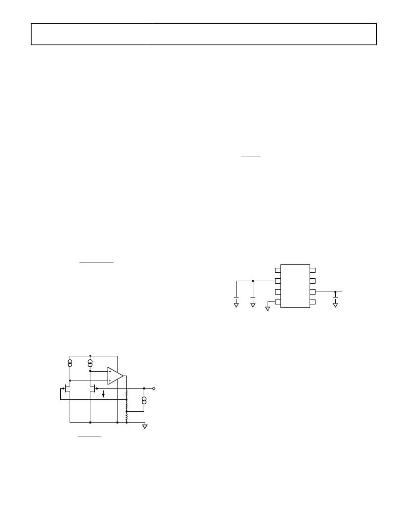
�The� simplified� schematic� in� Figure� 31� shows� the� basic� topology�
�of� the� ADR291/ADR292� series.� The� temperature� correction�
�term� is� provided� by� a� current� source� with� a� value� designed� to� be�
�proportional� to� absolute� temperature.� The� general� equation� is�
�where�
�T� J� and� T� A� are� the� junction� and� ambient� temperatures,�
�respectively.�
�P� D� is� the� device� power� dissipation.�
�θ� JA� is� the� device� package� thermal� resistance.�
�BASIC� VOLTAGE� REFERENCE� CONNECTIONS�
�References,� in� general,� require� a� bypass� capacitor� connected�
��illustrates� the� basic� configuration� for� the� ADR291/ADR292�
�family� of� references.� Note� that� the� decoupling� capacitors� are� not�
�?� +� (� I� PTAT� )� (� R� 3� )�
�V� OUT� =� Δ� V� P� ?�
�?� R� 1� +� R� 2� +� R� 3� ?�
�?� R� 1� ?�
�required� for� circuit� stability.�
�NC� 1�
�8�
�NC�
�where:�
�ΔV� P� is� the� difference� in� pinch-off� voltage� between� the� two� FETs.�
�I� PTAT� is� the� positive� temperature� coefficient� correction� current.�
�The� various� versions� of� the� ADR291/ADR292� family� are� created�
�+�
�10μF�
�0.1μF�
�NC�
�2�
�3�
�4�
�ADR291/�
�ADR292�
�7�
�6�
�5�
�NC�
�V� OUT�
�NC�
�0.1μF�
�by� on-chip� adjustment� of� R1� and� R3� to� achieve� 2.500� V� or�
�4.096� V� at� the� reference� output.�
�The� process� used� for� the� XFET� reference� also� features� vertical�
�NPN� and� PNP� transistors,� the� latter� of� which� are� used� as� output�
�devices� to� provide� a� very� low� dropout� voltage.�
�V� IN�
�NC� =� NO� CONNECT�
�Figure� 32.� Basic� Voltage� Reference� Configuration�
�NOISE� PERFORMANCE�
�The� noise� generated� by� the� ADR291/ADR292� family� of� refer-�
�ences� is� typically� less� than� 12� μV� p-p� over� the� 0.1� Hz� to� 10� Hz�
�band.� The� noise� measurement� is� made� with� a� band-pass� filter�
�I� 1�
�I� 1�
�made� of� a� 2-pole� high-pass� filter� with� a� corner� frequency� at� 0.1� Hz�
�and� a� 2-pole� low-pass� filter� with� a� corner� frequency� at� 10� Hz.�
�1�
� � V� P�
�R1�
�R2�
�V� OUT�
�I� PTAT�
�TURN-ON� TIME�
�Upon� application� of� power� (cold� start),� the� time� required� for�
�the� output� voltage� to� reach� its� final� value� within� a� specified�
�error� band� is� defined� as� the� turn-on� settling� time.� Two� com-�
�R3�
�ponents� normally� associated� with� this� are� the� time� it� takes� for�
�1� EXTRA�
�CHANNEL� IMPLANT�
�GND�
�the� active� circuits� to� settle� and� for� the� thermal� gradients� on� the�
�V� OUT� =�
�R1� +� R2� +� R3�
�R1�
�×� Δ� V� P� =� I� PTAT� ×� R3�
�chip� to� stabilize.� Figure� 28� shows� the� turn-on� settling� time� for�
�the� ADR291.�
�Figure� 31.� ADR291/ADR292� Simplified� Schematic�
�Rev.� F� |� Page� 13� of� 20�
�相关PDF资料 |
PDF描述 |
|---|---|
| A-MCUP-80050/R | CABLE CAT.5E UNSHIELDED RED 5M |
| UPB2W820MRD | CAP ALUM 82UF 450V 20% RADIAL |
| 0210490217 | CABLE JUMPER 1.25MM .102M 16POS |
| ESA10DTMH | CONN EDGECARD 20POS R/A .125 SLD |
| V375C2E50B3 | CONVERTER MOD DC/DC 2V 50W |
相关代理商/技术参数 |
参数描述 |
|---|---|
| ADR291FRZ-REEL7 | 功能描述:IC VREF SERIES PREC 2.5V 8-SOIC RoHS:是 类别:集成电路 (IC) >> PMIC - 电压基准 系列:XFET® 产品培训模块:Voltage Reference Basics 标准包装:100 系列:- 基准类型:旁路,精度 输出电压:4.096V 容差:±0.075% 温度系数:50ppm/°C 输入电压:- 通道数:1 电流 - 阴极:1µA 电流 - 静态:- 电流 - 输出:10mA 工作温度:0°C ~ 70°C 安装类型:表面贴装 封装/外壳:8-SOIC(0.154",3.90mm 宽) 供应商设备封装:8-SOIC 包装:管件 |
| ADR291GBC | 制造商:AD 制造商全称:Analog Devices 功能描述:Low Noise Micropower Precision Voltage References |
| ADR291GR | 制造商:Analog Devices 功能描述:V-Ref Precision 2.5V 5mA 8-Pin SOIC N Tube 制造商:Rochester Electronics LLC 功能描述:LOW NOISE MICROPWR PRECISION VOLT. REF. - Bulk 制造商:Analog Devices 功能描述:IC VOLT REF |
| ADR291GR-REEL | 制造商:Analog Devices 功能描述:V-Ref Precision 2.5V 5mA 8-Pin SOIC N T/R |
| ADR291GR-REEL7 | 制造商:Analog Devices 功能描述:V-Ref Precision 2.5V 5mA 8-Pin SOIC N T/R 制造商:Rochester Electronics LLC 功能描述:LOW NOISE MICROPWR PRECISION VOLT. REF. - Tape and Reel |
发布紧急采购,3分钟左右您将得到回复。