- 您现在的位置:买卖IC网 > PDF目录20698 > ADR435ARZ (Analog Devices Inc)IC VREF SERIES PREC 5V 8-SOIC PDF资料下载
参数资料
| 型号: | ADR435ARZ |
| 厂商: | Analog Devices Inc |
| 文件页数: | 16/24页 |
| 文件大小: | 0K |
| 描述: | IC VREF SERIES PREC 5V 8-SOIC |
| 产品培训模块: | Top Five Instrumentation Amplifier Problems |
| 设计资源: | Converting a Single-Ended Signal with AD7982 Differential PulSAR ADC (CN0032) Converting a Single-Ended Signal with AD7984 Differential PulSAR ADC (CN0033) Parametric Measurement Unit and Supporting Components for PAD Appls Using AD5522 and AD7685 (CN0104) Automated Calibration Technique That Reduces AD5360 Offset Voltage to Less Than 1 mV (CN0123) Integrated Device Power Supply for PAD with Output Voltage Range 0 V to 25 V (CN0130) 16 Channels of Programmable Output Span Using AD5360 (CN0131) 40 Channels of Programmable Output Span Using AD5371 (CN0149) Precision Single-Supply Differential ADC Driver for Industrial-Level Signals (CN0180) |
| 标准包装: | 98 |
| 系列: | XFET® |
| 基准类型: | 串联,精度 |
| 输出电压: | 5V |
| 容差: | ±0.12% |
| 温度系数: | 10ppm/°C |
| 输入电压: | 7 V ~ 18 V |
| 通道数: | 1 |
| 电流 - 静态: | 800µA |
| 电流 - 输出: | 30mA |
| 工作温度: | -40°C ~ 125°C |
| 安装类型: | 表面贴装 |
| 封装/外壳: | 8-SOIC(0.154",3.90mm 宽) |
| 供应商设备封装: | 8-SO |
| 包装: | 管件 |
| 产品目录页面: | 796 (CN2011-ZH PDF) |
�� ��
��
��ADR430/ADR431/ADR433/ADR434/ADR435/ADR439�
�THEORY� OF� OPERATION�
�The� ADR43x� series� of� references� uses� a� reference� generation�
�technique� known� as� XFET� (eXtra� implanted� junction� FET).�
�This� technique� yields� a� reference� with� low� supply� current,� good�
�thermal� hysteresis,� and� exceptionally� low� noise.� The� core� of� the�
�XFET� reference� consists� of� two� junction� field-effect� transistors�
�The� ADR43x� family� of� references� is� guaranteed� to� deliver� load�
�currents� to� 10� mA� with� an� input� voltage� that� ranges� from� 4.1� V�
�to� 18� V.� When� these� devices� are� used� in� applications� at� higher�
�currents,� use� the� following� equation� to� account� for� the�
�temperature� effects� due� to� the� power� dissipation� increases:�
�(JFETs),� one� of� which� has� an� extra� channel� implant� to� raise� its�
�T� J� =� P� D� ×� θ� JA� +� T� A�
�(2)�
�pinch-off� voltage.� By� running� the� two� JFETs� at� the� same� drain�
�current,� the� difference� in� pinch-off� voltage� can� be� amplified� and�
�used� to� form� a� highly� stable� voltage� reference.�
�The� intrinsic� reference� voltage� is� around� 0.5� V� with� a� negative�
�temperature� coefficient� of� about� ?120� ppm/°C.� This� slope� is�
�essentially� constant� to� the� dielectric� constant� of� silicon� and� can�
�be� compensated� closely� by� adding� a� correction� term� generated�
�in� the� same� fashion� as� the� proportional-to-temperature� (PTAT)�
�term� used� to� compensate� band� gap� references.� The� primary�
�advantage� of� an� XFET� reference� is� its� correction� term,� which� is�
�~30� times� lower� and� requires� less� correction� than� that� of� a� band�
�gap� reference.� Because� most� of� the� noise� of� a� band� gap� reference�
�where:�
�T� J� and� T� A� are� the� junction� and� ambient� temperatures,� respectively.�
�P� D� is� the� device� power� dissipation.�
�θ� JA� is� the� device� package� thermal� resistance.�
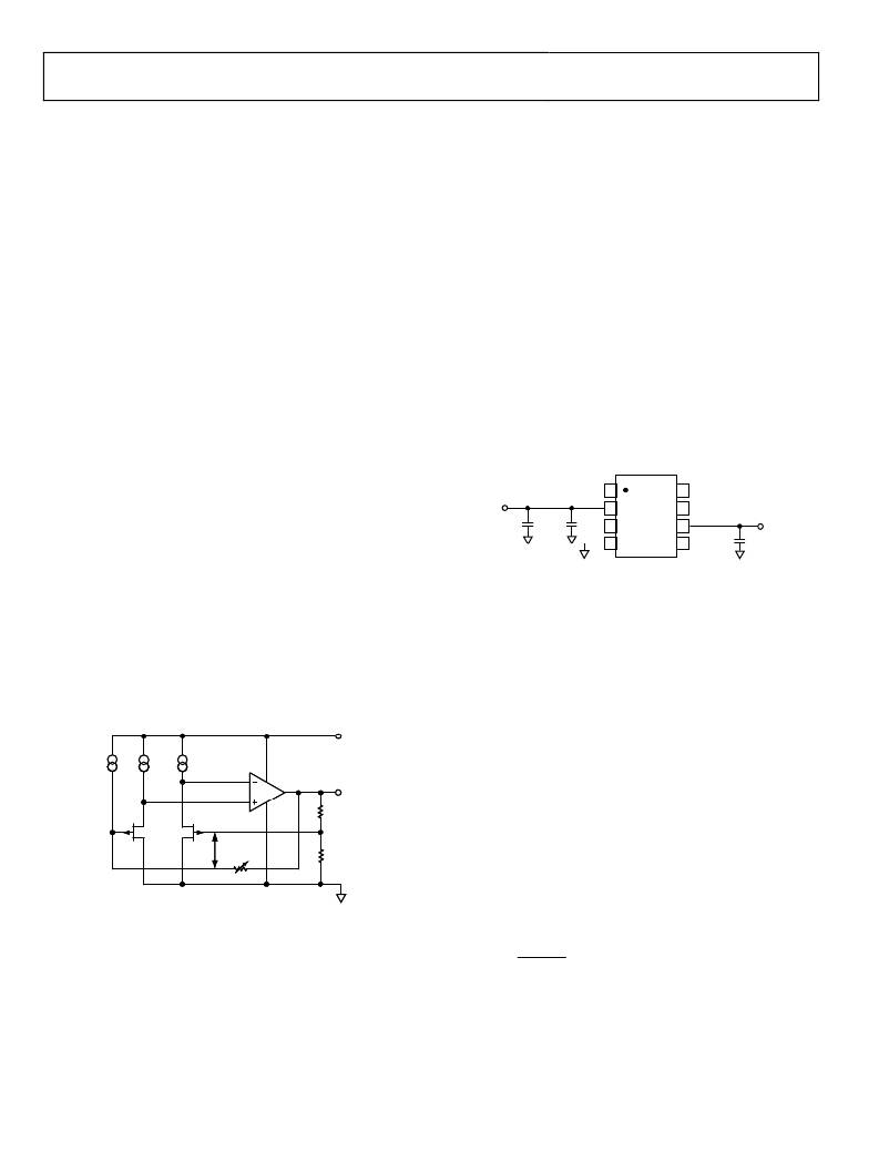
�BASIC� VOLTAGE� REFERENCE� CONNECTIONS�
�Voltage� references,� in� general,� require� a� bypass� capacitor�
��illustrates� the� basic� configuration� for� the� ADR43x� family�
�of� references.� Other� than� a� 0.1� μF� capacitor� at� the� output� to�
�help� improve� noise� suppression,� a� large� output� capacitor� at�
�the� output� is� not� required� for� circuit� stability.�
�TOP� VIEW�
�(Not� to� Scale)�
�comes� from� the� temperature� compensation� circuitry,� the� XFET�
�results� in� much� lower� noise.�
��temperature� correction� term� is� provided� by� a� current� source�
�V� IN�
�10μF�
�+�
�0.1μF�
�TP�
�NC�
�GND�
�1� 8�
�2� ADR43x� 7�
�3� 6�
�4� 5�
�TP�
�COMP�
�V� OUT�
�TRIM�
�0.1μF�
�with� a� value� designed� to� be� proportional� to� absolute� temperature.�
�The� general� equation� is�
�V� OUT� =� G� (� ΔV� P� –� R1� ×� I� PTAT� )�
�where:�
�G� is� the� gain� of� the� reciprocal� of� the� divider� ratio.�
�(1)�
�NOTES:�
�1.� NC� =� NO� CONNECT�
�2.� TP� =� TEST� PIN� (DO� NOT� CONNECT)�
�Figure� 30.� Basic� Voltage� Reference� Configuration�
�NOISE� PERFORMANCE�
�Δ� V� P� is� the� difference� in� pinch-off� voltage� between� the� two� JFETs.�
�I� PTAT� is� the� positive� temperature� coefficient� correction� current.�
�ADR43x� devices� are� created� by� on-chip� adjustment� of� R2� and� R3� to�
�achieve� 2.048� V� or� 2.500� V,� respectively,� at� the� reference� output.�
�V� IN�
�I� 1� I� 1�
�I� PTAT� ADR43x�
�V� OUT�
�R2�
�*�
�The� noise� generated� by� the� ADR43x� family� of� references� is�
�typically� less� than� 3.75� μV� p-p� over� the� 0.1� Hz� to� 10.0� Hz� band�
�for� ADR430,� ADR431,� and� ADR433.� Figure� 22� shows� the� 0.1� Hz�
�to� 10.0� Hz� noise� of� the� ADR431,� which� is� only� 3.5� μV� p-p.� The�
�noise� measurement� is� made� with� a� band-pass� filter� made� of� a�
�2-pole� high-pass� filter� with� a� corner� frequency� at� 0.1� Hz� and� a�
�2-pole� low-pass� filter� with� a� corner� frequency� at� 10.0� Hz.�
�HIGH� FREQUENCY� NOISE�
�The� total� noise� generated� by� the� ADR43x� family� of� references� is�
��?� V� P�
�R1�
�R3�
�shows� the� wideband� noise� from� 10� Hz� to� 25� kHz.� An� internal� node�
�of� the� op� amp� is� brought� out� on� Pin� 7,� and� by� overcompensating�
�the� op� amp,� the� overall� noise� can� be� reduced.�
�*EXTRA� CHANNEL� IMPLANT�
�V� OUT� =� G(� ?� V� P� –� R1� ×� I� PTAT� )�
�Figure� 29.� Simplified� Schematic� Device�
�GND�
�This� is� understood� by� considering� that� in� a� closed-loop�
�configuration,� the� effective� output� impedance� of� an� op� amp� is�
�Power� Dissipation� Considerations�
�R� O� =�
�r� O�
�1� +� A� VO� β�
�(3)�
�where:�
�R� O� is� the� apparent� output� impedance.�
�r� O� is� the� output� resistance� of� the� op� amp.�
�A� VO� is� the� open-loop� gain� at� the� frequency� of� interest.�
�β� is� the� feedback� factor.�
�Rev.� J� |� Page� 16� of� 24�
�相关PDF资料 |
PDF描述 |
|---|---|
| ECC12DRYI-S13 | CONN EDGECARD 24POS .100 EXTEND |
| EMC08DRES-S13 | CONN EDGECARD 16POS .100 EXTEND |
| RBC15DRXI | CONN EDGECARD 30POS DIP .100 SLD |
| HBC12DRTN | CONN EDGECARD 24POS DIP .100 SLD |
| HBC12DRTH | CONN EDGECARD 24POS DIP .100 SLD |
相关代理商/技术参数 |
参数描述 |
|---|---|
| ADR435ARZARZ | 制造商:Analog Devices 功能描述:ADR435A 5.0V voltage reference SOIC |
| ADR435ARZ-REEL7 | 功能描述:IC VREF SERIES PREC 5V 8-SOIC RoHS:是 类别:集成电路 (IC) >> PMIC - 电压基准 系列:XFET® 标准包装:2,000 系列:- 基准类型:旁路,可调节,精度 输出电压:1.24 V ~ 16 V 容差:±0.5% 温度系数:- 输入电压:1.24 V ~ 16 V 通道数:1 电流 - 阴极:100µA 电流 - 静态:- 电流 - 输出:20mA 工作温度:-40°C ~ 85°C 安装类型:通孔 封装/外壳:TO-226-3、TO-92-3(TO-226AA)成形引线 供应商设备封装:TO-92-3 包装:带卷 (TR) |
| ADR435B | 制造商:AD 制造商全称:Analog Devices 功能描述:Ultralow Noise XFET Voltage References with Current Sink and Source Capability |
| ADR435BR | 制造商:Analog Devices 功能描述:V-Ref Precision 5V 30mA 8-Pin SOIC N Tube |
| ADR435BRMZ | 功能描述:IC VREF SERIES PREC 5V 8-MSOP RoHS:是 类别:集成电路 (IC) >> PMIC - 电压基准 系列:XFET® 标准包装:1,000 系列:- 基准类型:旁路,可调节,精度 输出电压:2.495 V ~ 36 V 容差:±0.5% 温度系数:标准值 34ppm/°C 输入电压:2.495 V ~ 36 V 通道数:1 电流 - 阴极:1mA 电流 - 静态:- 电流 - 输出:100mA 工作温度:0°C ~ 70°C 安装类型:表面贴装 封装/外壳:TO-243AA 供应商设备封装:SOT-89-3 包装:带卷 (TR) |
发布紧急采购,3分钟左右您将得到回复。