- 您现在的位置:买卖IC网 > PDF目录20693 > ADR440BRZ (Analog Devices Inc)IC VREF SERIES PREC 2.048V 8SOIC PDF资料下载
参数资料
| 型号: | ADR440BRZ |
| 厂商: | Analog Devices Inc |
| 文件页数: | 14/20页 |
| 文件大小: | 0K |
| 描述: | IC VREF SERIES PREC 2.048V 8SOIC |
| 标准包装: | 98 |
| 系列: | XFET® |
| 基准类型: | 串联,精度 |
| 输出电压: | 2.048V |
| 容差: | ±0.05% |
| 温度系数: | 3ppm/°C |
| 输入电压: | 3 V ~ 18 V |
| 通道数: | 1 |
| 电流 - 静态: | 3.75mA |
| 电流 - 输出: | 10mA |
| 工作温度: | -40°C ~ 125°C |
| 安装类型: | 表面贴装 |
| 封装/外壳: | 8-SOIC(0.154",3.90mm 宽) |
| 供应商设备封装: | 8-SO |
| 包装: | 管件 |
| 产品目录页面: | 796 (CN2011-ZH PDF) |
�� ��
��
��ADR440/ADR441/ADR443/ADR444/ADR445�
�THEORY� OF� OPERATION�
�The� ADR44x� series� of� references� uses� a� new� reference� generation�
�technique� known� as� XFET� (eXtra� implanted� junction� FET).�
�This� technique� yields� a� reference� with� low� dropout,� good�
�thermal� hysteresis,� and� exceptionally� low� noise.� The� core� of� the�
�XFET� reference� consists� of� two� junction� field-effect� transistors�
�(JFETs),� one� of� which� has� an� extra� channel� implant� to� raise� its�
�POWER� DISSIPATION� CONSIDERATIONS�
�The� ADR44x� family� of� references� is� guaranteed� to� deliver� load�
�currents� to� 10� mA� with� an� input� voltage� that� ranges� from� 3� V� to�
�18� V.� When� these� devices� are� used� in� applications� at� higher�
�currents,� use� the� following� equation� to� account� for� the�
�temperature� effects� of� increases� in� power� dissipation:�
�pinch-off� voltage.� By� running� the� two� JFETs� at� the� same� drain�
�current,� the� difference� in� pinch-off� voltage� can� be� amplified�
�and� used� to� form� a� highly� stable� voltage� reference.�
�The� intrinsic� reference� voltage� is� around� 0.5� V� with� a� negative�
�temperature� coefficient� of� about� –120� ppm/°C.� This� slope� is�
�essentially� constant� to� the� dielectric� constant� of� silicon,� and� it� can�
�be� closely� compensated� for� by� adding� a� correction� term� generated�
�in� the� same� fashion� as� the� proportional-to-absolute� temperature�
�(PTAT)� term� used� to� compensate� band� gap� references.� The�
�advantage� of� an� XFET� reference� is� its� correction� term,� which� is�
�approximately� 20� times� lower� and� requires� less� correction� than�
�that� of� a� band� gap� reference.� Because� most� of� the� noise� of� a� band�
�gap� reference� comes� from� the� temperature� compensation�
�T� J� =� P� D� ×� θ� JA� +� T� A�
�where:�
�T� J� and� T� A� are� the� junction� and� ambient� temperatures,�
�respectively.�
�P� D� is� the� device� power� dissipation.�
�θ� JA� is� the� device� package� thermal� resistance.�
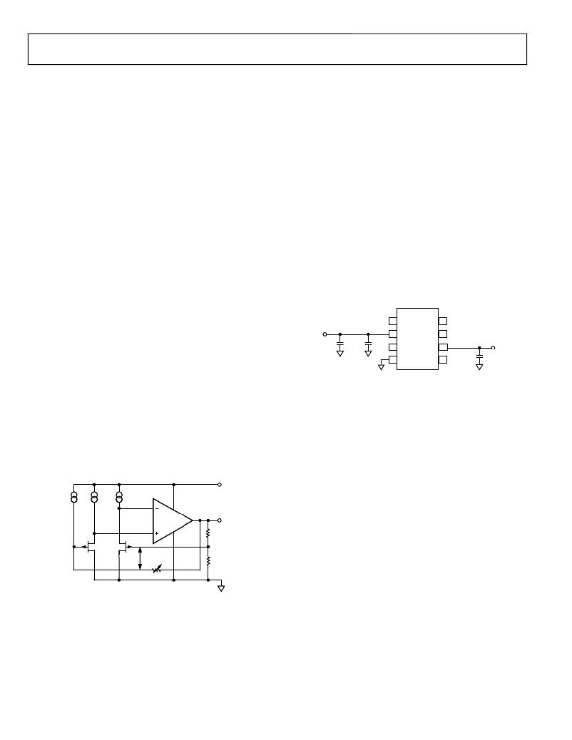
�BASIC� VOLTAGE� REFERENCE� CONNECTIONS�
�The� ADR44x� family� requires� a� 0.1� μF� capacitor� on� the� input�
�and� the� output� for� stability.� Although� not� required� for� operation,�
�a� 10� μF� capacitor� at� the� input� can� help� with� line� voltage�
�transient� performance.�
�(2)�
�circuitry,� the� XFET� results� in� much� lower� noise.�
�TP� 1�
�ADR440/�
�ADR441/�
�8�
�TP�
��temperature� correction� term� is� provided� by� a� current� source� with�
�V� IN�
�10μF�
�+�
�0.1μF�
�2�
�NC� 3�
�ADR443/�
�ADR444/�
�ADR445�
�7�
�6�
�NC�
�V� OUT�
�a� value� designed� to� be� proportional� to� the� absolute� temperature.�
�The� general� equation� is�
�NOTES�
�GND�
�4�
�TOP� VIEW�
�(Not� to� Scale)�
�5�
�TRIM�
�0.1μF�
�V� OUT� =� G� (Δ� V� P� ?� R1� ×� I� PTAT� )�
�(1)�
�1.� NC� =� NO� CONNECT�
�2.� TP� =� TEST� PIN� (DO� NOT� CONNECT)�
�where:�
�G� is� the� gain� of� the� reciprocal� of� the� divider� ratio.�
�Δ� V� P� is� the� difference� in� pinch-off� voltage� between� the� two� JFETs.�
�I� PTAT� is� the� positive� temperature� coefficient� correction� current.�
�ADR44x� devices� are� created� by� on-chip� adjustment� of� R2�
�and� R3� to� achieve� the� different� voltage� options� at� the�
�reference� output.�
�V� IN�
�Figure� 34.� Basic� Voltage� Reference� Configuration�
�NOISE� PERFORMANCE�
�The� noise� generated� by� the� ADR44x� family� of� references� is�
�typically� less� than� 1.4� μV� p-p� over� the� 0.1� Hz� to� 10.0� Hz� band�
�for� ADR440,� ADR441,� and� ADR443.� Figure� 26� shows� the� 0.1� Hz�
�to� 10� Hz� noise� of� the� ADR441,� which� is� only� 1.2� μV� p-p.� The�
�noise� measurement� is� made� with� a� band-pass� filter� composed� of�
�a� 2-pole� high-pass� filter� with� a� corner� frequency� at� 0.1� Hz� and� a�
�I� PTAT�
�I� 1�
�I� 1�
�ADR44x�
�V� OUT�
�2-pole� low-pass� filter� with� a� corner� frequency� at� 10.0� Hz.�
�TURN-ON� TIME�
�*�
�R2�
�Upon� application� of� power� (cold� start),� the� time� required� for�
�the� output� voltage� to� reach� its� final� value� within� a� specified�
�?� V� P�
�R1�
�R3�
�error� band� is� defined� as� the� turn-on� settling� time.� Two� compo-�
�nents� normally� associated� with� this� are� the� time� for� the� active�
�circuits� to� settle� and� the� time� for� the� thermal� gradients� on� the�
�*EXTRA� CHANNEL� IMPLANT�
�chip� to� stabilize.� Figure� 20� and� Figure� 21� show� the� turn-on� and�
�V� OUT� =� G� (� ?� V� P� –� R1� ×� I� PTAT� )�
�GND�
�turn-off� settling� times� for� the� ADR441.�
�Figure� 33.� Simplified� Schematic� Device�
�Rev.� E� |� Page� 14� of� 20�
�相关PDF资料 |
PDF描述 |
|---|---|
| EBM18DCWT | CONN EDGECARD 36POS DIP .156 SLD |
| ASM36DRKN | CONN EDGECARD 72POS DIP .156 SLD |
| ASM36DRKH | CONN EDGECARD 72POS DIP .156 SLD |
| ADR443BRZ | IC VREF SERIES PREC 3V 8-SOIC |
| AMM06DRES | CONN EDGECARD 12POS .156 EYELET |
相关代理商/技术参数 |
参数描述 |
|---|---|
| ADR440BRZ-REEL7 | 功能描述:IC VREF SERIES PREC 2.048V 8SOIC RoHS:是 类别:集成电路 (IC) >> PMIC - 电压基准 系列:XFET® 标准包装:2,000 系列:- 基准类型:旁路,可调节,精度 输出电压:1.24 V ~ 16 V 容差:±0.5% 温度系数:- 输入电压:1.24 V ~ 16 V 通道数:1 电流 - 阴极:100µA 电流 - 静态:- 电流 - 输出:20mA 工作温度:-40°C ~ 85°C 安装类型:通孔 封装/外壳:TO-226-3、TO-92-3(TO-226AA)成形引线 供应商设备封装:TO-92-3 包装:带卷 (TR) |
| ADR441 | 制造商:AD 制造商全称:Analog Devices 功能描述:2.048 V High Precision, LDO XFET® References for High Performance Sigma-Delta and PulSAR® Converters |
| ADR441A | 制造商:AD 制造商全称:Analog Devices 功能描述:Ultralow Noise, LDO XFET Voltage References with Current Sink and Source |
| ADR441AR | 制造商:Analog Devices 功能描述:V-REF PRECISION 2.5V 10MA 8SOIC N - Bulk |
| ADR441ARMZ | 功能描述:IC VREF SERIES PREC 2.5V 8-MSOP RoHS:是 类别:集成电路 (IC) >> PMIC - 电压基准 系列:XFET® 标准包装:3,000 系列:- 基准类型:旁路,精度 输出电压:3V 容差:±0.5% 温度系数:100ppm/°C 输入电压:- 通道数:1 电流 - 阴极:82µA 电流 - 静态:- 电流 - 输出:15mA 工作温度:-40°C ~ 85°C 安装类型:表面贴装 封装/外壳:6-TSSOP(5 引线),SC-88A,SOT-353 供应商设备封装:SC-70-5 包装:带卷 (TR) 其它名称:296-20888-2 |
发布紧急采购,3分钟左右您将得到回复。