- 您现在的位置:买卖IC网 > PDF目录375262 > ADS-CCD1201MC (CD TECHNOLOGIES INC) 12-Bit, 1.2MHz, Sampling A/D Optimized for CCD Appl PDF资料下载
参数资料
| 型号: | ADS-CCD1201MC |
| 厂商: | CD TECHNOLOGIES INC |
| 元件分类: | ADC |
| 英文描述: | 12-Bit, 1.2MHz, Sampling A/D Optimized for CCD Appl |
| 中文描述: | 1-CH 12-BIT FLASH METHOD ADC, PARALLEL ACCESS, DIP24 |
| 封装: | DDIP-24 |
| 文件页数: | 4/8页 |
| 文件大小: | 374K |
| 代理商: | ADS-CCD1201MC |
ADS -CCD1201
CALIBRATION PROCEDURE
(Refer to Figures 2 and 3)
Any offset and/or gain calibration procedures should not be
implemented until devices are fully warmed up. To avoid
interaction, offset must be adjusted before gain. The ranges of
adjustment for the circuit of Figure 2 are guaranteed to
compensate for the ADS-CCD1201’s initial accuracy errors and
may not be able to compensate for additional system errors.
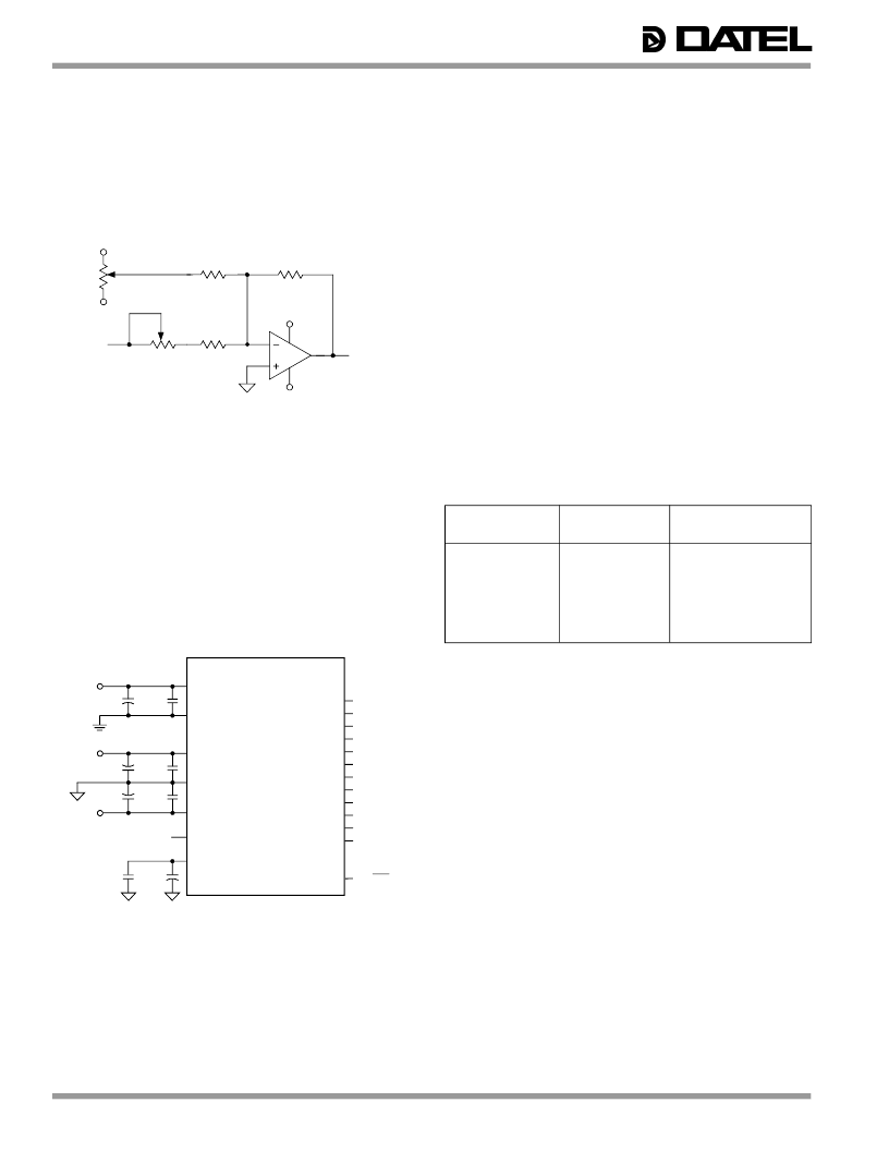
Figure 2. ADS-CCD1201 Calibration Circuit
All fixed resistors in Figure 2 should be metal-film types, and
multi-turn potentiometers should have TCR’s of 100ppm/°C or
less to minimize drift with temperature. In many applications,
the CCD will require an offset-adjust (black balance) circuit
near its output and also a gain stage, presumably with adjust
capabilities, to match the output voltage of the CCD to the
input range of the AID. If one is performing a "system I/O
calibration" (from light in to digital out), these circuits can be
used to compensate for the relatively small initial offset and
gain errors of the A/D. This would eliminate the need for the
circuit shown in Figure 2.
Figure 3. Typical ADS-CCD1201 Connection Diagram
A/D converters are calibrated by positioning their digital
outputs exactly on the transition point between two adjacent
digital output codes. This can be accomplished by connecting
LED’s to the digital outputs and adjusting until certain LED’s
"flicker" equally between on and off. Other approaches employ
digital comparators or microcontrollers to detect when the
outputs change from one code to the next.
For the ADS-CCD1201, offset adjusting is normally
accomplished at the point where all output bits are 0’s and the
LSB just changes from a 0 to a 1. This digital output transition
ideally occurs when the applied analog input is +1/2LSB
(+1.2207mV).
Gain adjusting is accomplished when all bits are 1’s and the
LSB just changes from a 1 to a 0. This transition ideally occurs
when the analog input is at +full scale minus 1 1/2 LSB’s
(+9.99634V).
Offset Adjust Procedure
1. Apply a train of pulses to the START CONVERT input (pin
16) so the converter is continuously converting. If using
LED’s on the outputs, a 200kHz conversion rate will reduce
flicker.
2. Apply +1.2207mV to the ANALOG INPUT (pin 20).
3. Adjust the offset potentiometer until the output bits are
0000 0000 00000 and the LSB flickers between 0 and 1.
Gain Adjust Procedure
1. Apply +9.99634V to the ANALOG INPUT (pin 20).
2. Adjust the gain potentiometer until all output bits are 1’s and
the LSB flickers between 1 and 0.
Table 2. ADS-CCD1201 Output Coding
Input Voltage
(0 to +10V)
Unipolar
Scale
Digital Output
MSB LSB
+9.9976
+7.5000
+5.0000
+2.5000
+0.0024
0
+FS – 1LSB
+3/4 FS
+1/2 FS
+1/4 FS
+1LSB
0
1111 1111 1111
1100 0000 0000
1000 0000 0000
0100 0000 0000
0000 0000 0001
0000 0000 0000
Coding is straight binary; 1LSB = 2.44mV
All DATEL sampling A/D converters are fully characterized and
specified over operating temperature (case) ranges of 0 to
+70°C and – 55 to +125°C. All room-temperature (T
A
= +25°C)
production testing is performed without the use of heat sinks or
forced-air cooling. Thermal impedance figures for each device
are listed in their respective specification tables.
These devices do not normally require heat sinks, however,
standard precautionary design and layout procedures should
be used to ensure devices do not overheat. The ground and
power planes beneath the package, as well as all pcb signal
runs to and from the device, should be as heavy as possible to
help conduct heat away from the package. Electrically-
insulating, thermally-conductive "pads" may be installed
underneath the package. Devices should be soldered to boards
rather than "socketed," and of course, minimal air flow over the
surface can greatly help reduce the package temperature.
In more severe ambient conditions, the package/junction
temperature of a given device can be reduced dramatically
(typically 35%) by using one of DATELs HS Series heat sinks.
See Ordering Information for the assigned part number. See
page 1-183 of the DATEL Data Acquisition Components
Catalog for more information on the HS Series. Request DATEL
Application Note AN-8, "Heat Sinks for DIP Data Converters,"or
contact DATEL directly, for additional information.
THERMAL REQUIREMENTS
4
.
To Pin 20 of
ADS-CCD1201
–15V
SIGNAL
INPUT
AGAIN
1.98k
50
+15V
2k
200k
20k
–15V
+15V
ZERO/
OFFSET
ADJUST
13
ADS-CCD1201
14
20
15
12
11
10
9
8
7
6
5
4
3
2
1
BIT 1 (MSB)
BIT 2
BIT 3
BIT 4
BIT 5
BIT 6
BIT 7
BIT 8
BIT 9
BIT 10
BIT 11
BIT 12 (LSB)
EOC
ANALOG
INPUT
19, 23
22
24
0.1μF
4.7μF
+5V
0.1μF
4.7μF
0.1μF
4.7μF
+
+
–12V/–15V
+12V/+15V
+
0.1μF
+
4.7μF
21 +10V REF. OUT
0 to +10V
NO CONNECT
17, 18
相关PDF资料 |
PDF描述 |
|---|---|
| ADS-CCD1201MM | 12-Bit, 1.2MHz, Sampling A/D Optimized for CCD Appl |
| ADS-EVAL4 | 14-Bit, 1MHz Sampling A/D Converters |
| ADS1203 | MOTOR CONTROL CURRENT MEASUREMENT |
| ADS1203IPWR | MOTOR CONTROL CURRENT MEASUREMENT |
| ADS1203IPWT | S/P 20 RED REV M |
相关代理商/技术参数 |
参数描述 |
|---|---|
| ADS-CCD1201MC-C | 制造商:Murata Power Solutions 功能描述: |
| ADS-CCD1201MM | 制造商:Murata Power Solutions 功能描述:ADC Single Flash 1.2Msps 12-bit Parallel 24-Pin DDIP |
| ADS-CCD1202 | 制造商:MURATA-PS 制造商全称:Murata Power Solutions Inc. 功能描述:12-Bit, 2MHz, Sampling A/D’s for CCD Imaging Applications |
| ADS-CCD1202MC | 功能描述:模数转换器 - ADC 0to+70C Unipolar A/D DDIP 1.75W12Bit 2MHz RoHS:否 制造商:Texas Instruments 通道数量:2 结构:Sigma-Delta 转换速率:125 SPs to 8 KSPs 分辨率:24 bit 输入类型:Differential 信噪比:107 dB 接口类型:SPI 工作电源电压:1.7 V to 3.6 V, 2.7 V to 5.25 V 最大工作温度:+ 85 C 安装风格:SMD/SMT 封装 / 箱体:VQFN-32 |
| ADS-CCD1202MM | 制造商:Murata Power Solutions 功能描述:ADC Single 2-Step Flash 2Msps 12-bit Parallel 24-Pin CDDIP |
发布紧急采购,3分钟左右您将得到回复。