- 您现在的位置:买卖IC网 > PDF目录375262 > ADS-EVAL4 (C) 14-Bit, 1MHz Sampling A/D Converters PDF资料下载
参数资料
| 型号: | ADS-EVAL4 |
| 厂商: | C |
| 元件分类: | 串行ADC |
| 英文描述: | 14-Bit, 1MHz Sampling A/D Converters |
| 中文描述: | 14位,1MHz的采样A / D转换器 |
| 文件页数: | 3/6页 |
| 文件大小: | 86K |
| 代理商: | ADS-EVAL4 |
ADS -941
3
TECHNICAL NOTES
1. Rated performance requires using good high-frequency
circuit board layout techniques. The analog and digital
grounds are not connected to each other internally. Avoid
ground-related problems by connecting the digital and
analog grounds to one point, the ground plane beneath the
converter. Due to the inductance and resistance of the
power supply return paths, return the analog and digital
ground separately to the power supplies.
2. Bypass the analog and digital supplies and the +10V REF.
OUT (pin 1) to ground with a 4.7μF, 25V tantalum electro-
lytic capacitor in parallel with a 0.1μF ceramic capacitor.
3. CODING SELECT (pin 8) is compatible with CMOS/TTL
logic levels for those users desiring logic control of this
function. The device has an internal pull-up resistor on this
pin, allowing pin 8 to be connected to +5V or left open when
a logic 1 is needed. See the Calibration Procedure for
selecting an output coding.
4. To enable the three-state outputs, connect ENABLE (pin 9)
to a logic "0" (low). To disable, connect pin 9 to a logic "1"
(high).
CALIBRATION PROCEDURE
1. Connect the converter per Figure 3 and Table 1 for the
appropriate input range. Apply a pulse of 50 nanoseconds
minimum to START CONVERT (pin 32) at a rate of 200kHz.
This rate is chosen to reduce flicker if LED's are used on
the outputs for calibration purposes.
2.
Zero Adjustments
Apply a precision voltage reference source between
ANALOG INPUT (pin 3) and SIGNAL GROUND (pin 4),
then adjust the reference source output per Table 2.
For unipolar operation, adjust the zero trimpot so that the
output code flickers equally between 00 0000 0000 0000
and 00 0000 0000 0001 with CODING SELECT (pin 8) tied
low (straight binary) or between 11 1111 1111 1111 and 11
1111 1111 1110 with pin 8 tied high (complementary binary).
For bipolar operation, adjust the trimpot until the code
flickers equally between 10 0000 0000 0000 and 10 0000
0000 0001 with pin 8 tied low (offset binary) or between 01
1111 1111 1111 and 01 1111 1111 1110 with pin 8 tied high
(complementary offset binary).
Two's complement coding requires using BIT 1 OUT (MSB)
(pin 31). With pin 8 tied low, adjust the trimpot until the
code flickers between 00 0000 0000 0000 and 00 0000
0000 0001.
3.
Full-Scale Adjustment
Set the output of the voltage reference used in step 2 to the
value shown in Table 2.
Adjust the gain trimpot until the output code flickers equally
between 11 1111 1111 1110 and 11 1111 1111 1111 with pin 8
THERMAL REQUIREMENTS
All DATEL sampling A/D converters are fully characterized and
specified over operating temperature (case) ranges of 0 to
+70°C and –55 to +125°C. All room-temperature (T
A
= +25°C)
production testing is performed without the use of heat sinks or
forced-air cooling. Thermal impedance figures for each device
are listed in their respective specification tables.
These devices do not normally require heat sinks, however,
standard precautionary design and layout procedures should
be used to ensure devices do not overheat. The ground and
power planes beneath the package, as well as all pcb signal
runs to and from the device, should be as heavy as possible to
help conduct heat away from the package. Electrically-
insulating, thermally-conductive "pads" may be installed
underneath the package. Devices should be soldered to
boards rather than "socketed", and of course, minimal air flow
over the surface can greatly help reduce the package
temperature.
In more severe ambient conditions, the package/junction
temperature of a given device can be reduced dramatically
(typically 35%) by using one of DATEL's HS Series heat sinks.
See Ordering Information for the assigned part number. See
page 1-183 of the DATEL Data Acquisition Components
Catalog for more information on the HS Series. Request
DATEL Application Note AN-8, "Heat Sinks for DIP Data
Converters", or contact DATEL directly, for additional
information.
tied low for straight binary/offset binary or between 00 0000
0000 0000 and 00 0000 0000 0001 with pin 8 tied high for
complementary binary/complementary offset binary.
Two's complement coding requires using pin 31. With pin 8
tied low, adjust the gain trimpot until the output code flickers
equally between 01 1111 1111 1110 and 01 1111 1111 1111.
4. To confirm proper operation of the device, vary the precision
reference voltage source to obtain the output coding listed
in Table 3.
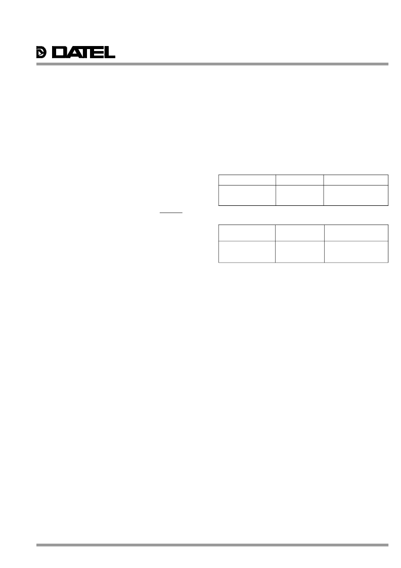
INPUT RANGE
INPUT PIN
TIE TOGETHER
0 +10V
±5V
Pin 3
Pin 3
Pins 2 and 4
Pins 1 and 2
Input
Range
Zero Adjust
+1/2 LSB
Gain Adjust
FS – 1 1/2 LSB
0 to +10V
±5V
+305μV
+305μV
+9.999085V
+4.999085V
Table 2. Zero and Gain Adjustments
Table 1. Input Connections
相关PDF资料 |
PDF描述 |
|---|---|
| ADS1203 | MOTOR CONTROL CURRENT MEASUREMENT |
| ADS1203IPWR | MOTOR CONTROL CURRENT MEASUREMENT |
| ADS1203IPWT | S/P 20 RED REV M |
| ADS1217 | 8-Channel, 24-Bit ANALOG-TO-DIGITAL CONVERTER |
| ADS1217IPFBR | 8-Channel, 24-Bit ANALOG-TO-DIGITAL CONVERTER |
相关代理商/技术参数 |
参数描述 |
|---|---|
| A-DSF 09LPIII/Z | 制造商:Assmann Electronics Inc 功能描述:Old Part A-DSF 09LPIII/Z^ASSMANN |
| A-DSF 25LPIII/Z-UNC | 制造商:Assmann Electronics Inc 功能描述: |
| A-DSF 37LPIII/FP | 功能描述:CONN DSUB PLUG 37POS STR IDC 制造商:assmann wsw components 系列:* 零件状态:有效 标准包装:32 |
| ADS-F09A-GTAXB7-R | 功能描述:CONN D-SUB STACKED M/F 9POS R/A RoHS:是 类别:连接器,互连式 >> D-Sub 系列:- 标准包装:20 系列:DM HE501 连接器类型:D-Sub 位置数:25 行数:2 外壳尺寸,连接器布局:3(DB,B) 触点类型::信号 连接器类型:插头,公引脚 安装类型:通孔,直角 法兰特点:配接侧;母型螺钉锁(4-40) 端子:焊接 特点:- 外壳材料,表面处理:钢,镀镉 触点表面涂层:金 触点涂层厚度:- 防护等级:- 工作温度:-55°C ~ 125°C 额定电压:- 额定电流:7.5A 体座材料:热塑塑胶,玻璃纤维增强型 颜色:- |
| A-DSF09LPIII/FP | 制造商:Assmann 功能描述:9w plastic IDC plug class III |
发布紧急采购,3分钟左右您将得到回复。