- 您现在的位置:买卖IC网 > PDF目录17096 > ADS1241MEVM (Texas Instruments)EVALUATION MODULE FOR ADS1241M PDF资料下载
参数资料
| 型号: | ADS1241MEVM |
| 厂商: | Texas Instruments |
| 文件页数: | 6/30页 |
| 文件大小: | 0K |
| 描述: | EVALUATION MODULE FOR ADS1241M |
| 产品培训模块: | Data Converter Basics |
| 视频文件: | Nuts and Bolts of the Delta-Sigma Converter |
| 标准包装: | 1 |
| ADC 的数量: | 1 |
| 位数: | 24 |
| 采样率(每秒): | 15 |
| 数据接口: | SPI? |
| 输入范围: | 0 ~ 2.5 V |
| 在以下条件下的电源(标准): | 0.6mW @ 3V |
| 工作温度: | -40°C ~ 85°C |
| 已用 IC / 零件: | ADS1241M |
| 已供物品: | 板 |
| 产品目录页面: | 889 (CN2011-ZH PDF) |
| 相关产品: | ADS1241EG4-ND - IC ADC 24-BIT SER PROGBL 28-SSOP ADS1241E/1KG4-ND - IC ADC 24-BIT SER PROGBL 28-SSOP 296-25895-2-ND - IC ADC 24-BIT SER PROGBL 28-SSOP ADS1241E-ND - IC ADC 24-BIT SER PROGBL 28-SSOP |
| 其它名称: | 296-18358 |
第1页第2页第3页第4页第5页当前第6页第7页第8页第9页第10页第11页第12页第13页第14页第15页第16页第17页第18页第19页第20页第21页第22页第23页第24页第25页第26页第27页第28页第29页第30页
ADS1240, 1241
14
SBAS173F
www.ti.com
Data Continuous Mode (RDATAC) command should not be
issued when DIN and DOUT are connected. While in RDATAC
mode, DIN looks for the STOPC or RESET command. If
either of these 8-bit bytes appear on DOUT (which is con-
nected to DIN), the RDATAC mode ends.
DATA READY DRDY PIN
The DRDY line is used as a status signal to indicate when
data is ready to be read from the internal data register.
DRDY goes LOW when a new data word is available in the
DOR register. It is reset HIGH when a read operation from
the data register is complete. It also goes HIGH prior to the
updating of the output register to indicate when not to read
from the device to ensure that a data read is not attempted
while the register is being updated.
The status of DRDY can also be obtained by interrogating bit
7 of the ACR register (address 2H). The serial interface can
operate in 3-wire mode by tying the CS input LOW. In this
case, the SCLK, DIN, and DOUT lines are used to communi-
cate with the ADS1240 and ADS1241. This scheme is
suitable for interfacing to microcontrollers. If CS is required
as a decoding signal, it can be generated from a port bit of
the microcontroller.
DSYNC OPERATION
Synchronization can be achieved either through the DSYNC
pin or the DSYNC command. When the DSYNC pin is used,
the digital circuitry is reset on the falling edge of DSYNC.
While DSYNC is LOW, the serial interface is deactivated.
Reset is released when DSYNC is taken HIGH. Synchroni-
zation occurs on the next rising edge of the system clock
after DSYNC is taken HIGH.
When the DSYNC command is sent, the digital filter is reset
on the edge of the last SCLK of the DSYNC command. The
modulator is held in RESET until the next edge of SCLK is
detected. Synchronization occurs on the next rising edge of
the system clock after the first SCLK following the DSYNC
command.
POWER-UP—SUPPLY VOLTAGE RAMP RATE
The power-on reset circuitry was designed to accommodate
digital supply ramp rates as slow as 1V/10ms. To ensure
proper operation, the power supply should ramp monotoni-
cally.
RESET
The user can reset the registers to their default values in
three different ways: by asserting the RESET pin; by issuing
the RESET command; or by applying a special waveform on
the SCLK (the
SCLK Reset Waveform, as shown in the
Timing Diagram). Note: if both POL and SCLK pins are held
high, applying the SCLK Reset Waveform to the CS pin also
resets the part.
logic one or zero when configured as an input to prevent
excess current dissipation. If the pin is configured as an
output in the DIR register, then the corresponding DIO
register bit value determines the state of the output pin
(0 = AGND, 1 = AVDD).
It is still possible to perform A/D conversions on a pin
configured as data I/O. This may be useful as a test mode,
where the data I/O pin is driven and an A/D conversion is
done on the pin.
SERIAL PERIPHERAL INTERFACE
The Serial Peripheral Interface (SPI) allows a controller to
communicate synchronously with the ADS1240 and ADS1241.
The ADS1240 and ADS1241 operate in slave-only mode.
The serial interface is a standard four-wire SPI (CS , SCLK,
DIN and DOUT) interface that supports both serial clock
polarities (POL pin).
Chip Select (CS )
The chip select (CS ) input must be externally asserted
before communicating with the ADS1240 or ADS1241. CS
must stay LOW for the duration of the communication.
Whenever CS goes HIGH, the serial interface is reset. CS
may be hard-wired LOW.
Serial Clock (SCLK)
The serial clock (SCLK) features a Schmitt-triggered input
and is used to clock DIN and DOUT data. Make sure to have
a clean SCLK to prevent accidental double-shifting of the
data. If SCLK is not toggled within 3 DRDY pulses, the serial
interface resets on the next SCLK pulse and starts a new
communication cycle. A special pattern on SCLK resets the
entire chip; see the RESET section for additional information.
Clock Polarity (POL)
The clock polarity input (POL) controls the polarity of SCLK.
When POL is LOW, data is clocked on the falling edge of
SCLK and SCLK should be idled LOW. Likewise, when POL
is HIGH, the data is clocked on the rising edge of SCLK and
SCLK should be idled HIGH.
Data Input (DIN) and Data Output (DOUT)
The data input (DIN) and data output (DOUT) receive and send
data from the ADS1240 and ADS1241. DOUT is high imped-
ance when not in use to allow DIN and DOUT to be connected
together and driven by a bidirectional bus. Note: the Read
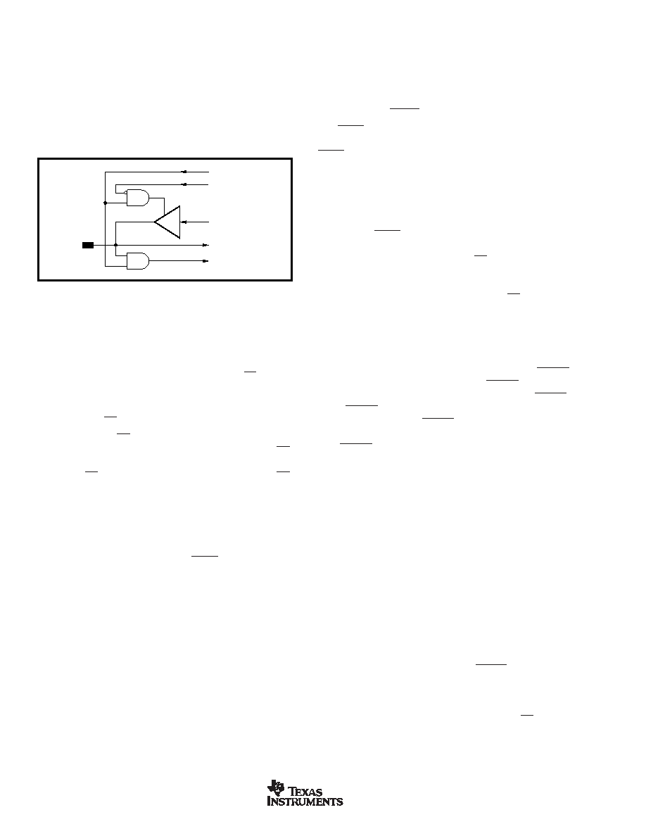
FIGURE 7. Analog/Data Interface Pin.
IOCON
A
INx/Dx
To Analog Mux
DIO WRITE
DIR
DIO READ
相关PDF资料 |
PDF描述 |
|---|---|
| SDR-VL | SCOTCH CODE REFILL VIOLET |
| FPF2302MX | IC LOAD SW 2CH LATCH-OFF 8-SOP |
| SCRH124-331 | INDUCTOR SMD 330UH 0.50A100KHZ |
| HW-V5-ML506-UNI-G-J | EVALUATION PLATFORM VIRTEX-5 |
| RCB06DHLT | CONN EDGECARD 12POS DIP .050 SLD |
相关代理商/技术参数 |
参数描述 |
|---|---|
| ADS1242 | 制造商:TI 制造商全称:Texas Instruments 功能描述:24-Bit ANALOG-TO-DIGITAL CONVERTER |
| ADS1242IPW | 制造商:Texas Instruments 功能描述:IC 24BIT ADC SMD 1242 TSSOP16 制造商:Texas Instruments 功能描述:IC, 24BIT ADC, SMD, 1242, TSSOP16 |
| ADS1242IPW | 制造商:Texas Instruments 功能描述:IC 24BIT ADC SMD 1242 TSSOP16 |
| ADS1242IPWR | 功能描述:模数转换器 - ADC 24-Bit ADC 4 Ch RoHS:否 制造商:Texas Instruments 通道数量:2 结构:Sigma-Delta 转换速率:125 SPs to 8 KSPs 分辨率:24 bit 输入类型:Differential 信噪比:107 dB 接口类型:SPI 工作电源电压:1.7 V to 3.6 V, 2.7 V to 5.25 V 最大工作温度:+ 85 C 安装风格:SMD/SMT 封装 / 箱体:VQFN-32 |
| ADS1242IPWRG4 | 功能描述:模数转换器 - ADC 24-Bit ADC 4 Ch RoHS:否 制造商:Texas Instruments 通道数量:2 结构:Sigma-Delta 转换速率:125 SPs to 8 KSPs 分辨率:24 bit 输入类型:Differential 信噪比:107 dB 接口类型:SPI 工作电源电压:1.7 V to 3.6 V, 2.7 V to 5.25 V 最大工作温度:+ 85 C 安装风格:SMD/SMT 封装 / 箱体:VQFN-32 |
发布紧急采购,3分钟左右您将得到回复。