- 您现在的位置:买卖IC网 > PDF目录10719 > ADS1286P (Texas Instruments)IC 12-BIT SAMPLING A/D 8-DIP PDF资料下载
参数资料
| 型号: | ADS1286P |
| 厂商: | Texas Instruments |
| 文件页数: | 2/17页 |
| 文件大小: | 0K |
| 描述: | IC 12-BIT SAMPLING A/D 8-DIP |
| 产品培训模块: | Data Converter Basics |
| 标准包装: | 50 |
| 位数: | 12 |
| 采样率(每秒): | 20k |
| 数据接口: | 串行,SPI?,SSI |
| 转换器数目: | 1 |
| 电压电源: | 单电源 |
| 工作温度: | 0°C ~ 70°C |
| 安装类型: | 通孔 |
| 封装/外壳: | 8-DIP(0.300",7.62mm) |
| 供应商设备封装: | 8-PDIP |
| 包装: | 管件 |
| 输入数目和类型: | 1 个差分,单极 |
| 产品目录页面: | 890 (CN2011-ZH PDF) |
10
ADS1286
MINIMIZING POWER DISSIPATION
In systems that have significant time between conversions,
the lowest power drain will occur with the minimum CS
LOW time. Bringing CS LOW, transferring data as quickly
as possible, and then bringing it back HIGH will result in the
lowest current drain. This minimizes the amount of time the
device draws power. After a conversion the A/D automati-
cally shuts down even if CS is held LOW. If the clock is left
running to clock out LSB-data or zero, the logic will draw a
small amount of current (see Figure 3).
REDUCED REFERENCE
OPERATION
The effective resolution of the ADS1286 can be increased
by reducing the input span of the converter. The ADS1286
exhibits good linearity and gain over a wide range of
reference voltages (see Typical Performance Curves “ Change
in Linearity vs Reference Voltage” and “Change in Gain vs
Reference Voltage”). However, care must be taken when
operating at low values of VREF because of the reduced LSB
size and the resulting higher accuracy requirement placed on
the converter. The following factors must be considered
when operating at low VREF values:
1. Offset
2. Noise
OFFSET WITH REDUCED V
REF
The offset of the ADS1286 has a larger effect on the output
code. When the ADC is operated with reduced reference
voltage. The offset (which is typically a fixed voltage)
becomes a larger fraction of an LSB as the size of the LSB
is reduced. The Typical Performance Curve “Change in
Offset vs Reference Voltage” shows how offset in LSBs is
related to reference voltage for a typical value of VOS. For
example, a VOS of 122V which is 0.1 LSB with a 5V
reference becomes 0.5LSB with a 1V reference and 2.5LSBs
with a 0.2V reference. If this offset is unacceptable, it can be
corrected digitally by the receiving system or by offsetting
the negative input of the ADS1286.
NOISE WITH REDUCED V
REF
The total input referred noise of the ADS1286 can be
reduced to approximately 200
V peak-to-peak using a ground
plane, good bypassing, good layout techniques and minimiz-
ing noise on the reference inputs. This noise is insignificant
with a 5V reference but will become a larger fraction of an
LSB as the size of the LSB is reduced.
For operation with a 5V reference, the 200
V noise is only
0.15LSB peak-to-peak. In this case, the ADS1286 noise will
contribute virtually no uncertainty to the output code. How-
ever, for reduced references, the noise may become a signifi-
cant fraction of an LSB and cause undesirable jitter in the
output code. For example, with a 2.5V reference this same
200
V noise is 0.3LSB peak-to-peak. If the reference is
further reduced to 1V, the 200
V noise becomes equal to
0.8LSBs and a stable code may be difficult to achieve. In
this case averaging multiple readings may be necessary.
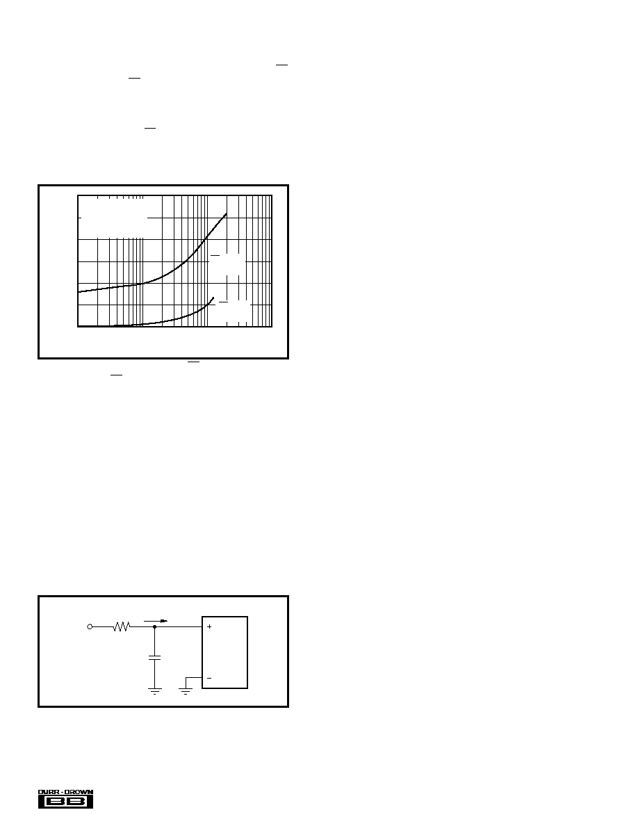
FIGURE 3. Shutdown Current with CS HIGH is Lower than
with CS LOW.
RC INPUT FILTERING
It is possible to filter the inputs with an RC network as
shown in Figure 4. For large values of CFILTER (e.g., 1F),
the capacitive input switching currents are averaged into a
net DC current. Therefore, a filter should be chosen with a
small resistor and large capacitor to prevent DC drops across
the resistor. The magnitude of the DC current is approxi-
mately IDC = 20pF x VIN/tCYC and is roughly proportional to
VIN. When running at the minimum cycle time of 64s, the
input current equals 1.56
A at V
IN = 5V. In this case, a filter
resistor of 75
will cause 0.1LSB of full-scale error. If a
larger filter resistor must be used, errors can be eliminated
by increasing the cycle time.
FIGURE 4. RC Input Filtering.
R
FILTER
I
DC
ADS1286
C
FILTER
V
IN
6.00
5.00
4.00
3.00
2.00
1.00
0.00
Supply
Current
(
A)
0.1
1
10
100
Sample Rate (kHz)
T
A = 25°C
V
CC = +5V
V
REF = +5V
f
CLK = 16 fSAMPLE
CS = LOW
(GND)
CS HIGH
(V
CC)
相关PDF资料 |
PDF描述 |
|---|---|
| VE-B6T-IV | CONVERTER MOD DC/DC 6.5V 150W |
| VI-B5Z-MX-B1 | CONVERTER MOD DC/DC 2V 30W |
| MCP6548T-E/SN | IC COMP 1.6V SNGL O-D W/CS 8SOIC |
| MCP6548T-I/SN | IC COMP OPENDRN 1.6V SNGL 8-SOIC |
| VI-B5Z-MW-B1 | CONVERTER MOD DC/DC 2V 40W |
相关代理商/技术参数 |
参数描述 |
|---|---|
| ADS1286P | 制造商:Texas Instruments 功能描述:IC 12BIT ADC 200 KHZ PDIP8 1286 |
| ADS1286PA | 功能描述:模数转换器 - ADC 12bit 200KHz Unipol RoHS:否 制造商:Texas Instruments 通道数量:2 结构:Sigma-Delta 转换速率:125 SPs to 8 KSPs 分辨率:24 bit 输入类型:Differential 信噪比:107 dB 接口类型:SPI 工作电源电压:1.7 V to 3.6 V, 2.7 V to 5.25 V 最大工作温度:+ 85 C 安装风格:SMD/SMT 封装 / 箱体:VQFN-32 |
| ADS1286PA | 制造商:BURR-BROWN 功能描述:IC 12BIT ADC 1286 DIP8 制造商:Texas Instruments 功能描述:Analog-Digital Converter IC Number of Bi |
| ADS1286PAG4 | 功能描述:模数转换器 - ADC 12B Micro Pwr Sampling ADC RoHS:否 制造商:Texas Instruments 通道数量:2 结构:Sigma-Delta 转换速率:125 SPs to 8 KSPs 分辨率:24 bit 输入类型:Differential 信噪比:107 dB 接口类型:SPI 工作电源电压:1.7 V to 3.6 V, 2.7 V to 5.25 V 最大工作温度:+ 85 C 安装风格:SMD/SMT 封装 / 箱体:VQFN-32 |
| ADS1286PB | 功能描述:模数转换器 - ADC 12-Bit Micro Power Sampling RoHS:否 制造商:Texas Instruments 通道数量:2 结构:Sigma-Delta 转换速率:125 SPs to 8 KSPs 分辨率:24 bit 输入类型:Differential 信噪比:107 dB 接口类型:SPI 工作电源电压:1.7 V to 3.6 V, 2.7 V to 5.25 V 最大工作温度:+ 85 C 安装风格:SMD/SMT 封装 / 箱体:VQFN-32 |
发布紧急采购,3分钟左右您将得到回复。