- 您现在的位置:买卖IC网 > PDF目录165354 > ADS5103 (Texas Instruments, Inc.) "10 Bit PDF资料下载
参数资料
| 型号: | ADS5103 |
| 厂商: | Texas Instruments, Inc. |
| 英文描述: | "10 Bit |
| 中文描述: | 具有关断状态、内部/外部参考的 10 位 40MSPS ADC |
| 文件页数: | 9/23页 |
| 文件大小: | 334K |
| 代理商: | ADS5103 |
ADS5102
ADS5103
SLAS351B – OCTOBER 2001 – REVISED DECEMBER 2001
17
www.ti.com
PRINCIPLES OF OPERATION
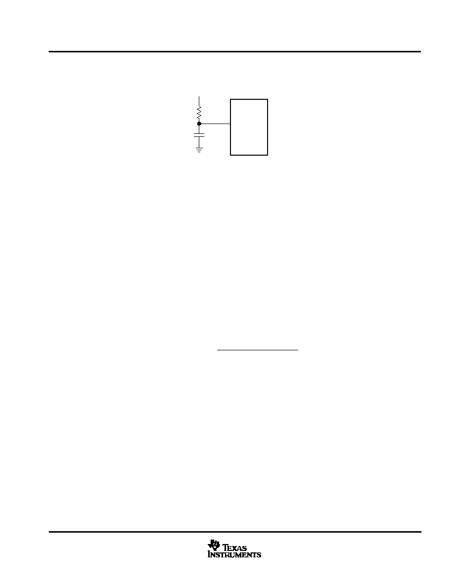
100 k
BG
1
F
AVDD
Figure 30. BG Reference Configuration
For systems that require more absolute accuracy or lower temperature coefficient drift than provided by the
internal VREF, an external voltage reference can be applied to the VREFB and VREFT inputs. To use external
reference, connect the PDREF pin to a logic high and this internally disconnects the VREF from the ADC. In
this mode it is also necessary to connect the BG and REFT pins together on the PWB. It is recommended to
use the input levels of VREFB = 0.75 V and VREFB = 1.25 V to achieve optimum ADC performance. It is also
recommended to apply a common-mode voltage to the input of 1 V.
clock input
The clock input is designed for 1.8 V or 3.3 V CMOS logic levels (depends on DRVDD) and it is recommended
to use standard CMOS logic levels as inputs. The logic threshold internally is set to DRVDD/2 or nominally 1.65
V. Since both edges of the clock are used in the switch capacitor architecture, it is important to provide a clock
with (ideally) a 50% duty cycle. The performance variation with clock duty cycle can be examined from
Figures 25, 26, 27 and 28.
Clock jitter is also important for performance of the ADC to be maintained. Any clock jitter appears as noise when
sampling input frequencies. Clock Jitter reduces the signal to noise ratio (SNR) and is more severe as the input
frequency increases. The theoretical SNR limits based on clock jitter can be calculated as follows:
Theoretical SNR
(clock jitter)
(dB)
+ 20 log
1
2
p
F
I
CLK
(jitter)
Where:
FI = Highest input frequency to the ADC in Hz
CLK(jitter) = the amount of jitter on the clock in sec
Therefore for a Nyquist frequency input of 32.5 MHz and a design trying to achieve the most available
performance from the ADS5102/3, the clock jitter must be less than 3.98 ps rms. In under sampling applications,
the same equations apply and clock jitter becomes more critical and may be the limiting factor in system
performance. The aperture jitter of the SHA also contributes to overall jitter. For worst case designs, the jitter
of clock and aperture can be considered to add in quadrature, i.e.
Total Jitter = Square root of ( CLKjitter2 + Aperturejitter 2)
The aperture jitter of the ADS5103 is 2 ps rms and at frequencies approaching Nyquist, the total jitter should
be accounted for.
相关PDF资料 |
PDF描述 |
|---|---|
| ADS5103CPFB | 1.8-V ANALOG SUPPLY, 10-BIT, 65/40 MSPS ANALOG-TO-DIGITAL CONVERTERS WITH INTERNAL REFERENCE |
| ADS5103CPFBR | 1.8-V ANALOG SUPPLY, 10-BIT, 65/40 MSPS ANALOG-TO-DIGITAL CONVERTERS WITH INTERNAL REFERENCE |
| ADS5103EVM | 1.8-V ANALOG SUPPLY, 10-BIT, 65/40 MSPS ANALOG-TO-DIGITAL CONVERTERS WITH INTERNAL REFERENCE |
| ADS5103IPFB | 1.8-V ANALOG SUPPLY, 10-BIT, 65/40 MSPS ANALOG-TO-DIGITAL CONVERTERS WITH INTERNAL REFERENCE |
| ADS5103IPFBR | 1.8-V ANALOG SUPPLY, 10-BIT, 65/40 MSPS ANALOG-TO-DIGITAL CONVERTERS WITH INTERNAL REFERENCE |
相关代理商/技术参数 |
参数描述 |
|---|---|
| ADS5103CPFB | 功能描述:模数转换器 - ADC 10 Bit 40MSPS 1.8V Int/Ext Ref w/Pwrdwn RoHS:否 制造商:Texas Instruments 通道数量:2 结构:Sigma-Delta 转换速率:125 SPs to 8 KSPs 分辨率:24 bit 输入类型:Differential 信噪比:107 dB 接口类型:SPI 工作电源电压:1.7 V to 3.6 V, 2.7 V to 5.25 V 最大工作温度:+ 85 C 安装风格:SMD/SMT 封装 / 箱体:VQFN-32 |
| ADS5103CPFBG4 | 功能描述:模数转换器 - ADC 10 Bit 40MSPS 1.8V Int/Ext Ref w/Pwrdwn RoHS:否 制造商:Texas Instruments 通道数量:2 结构:Sigma-Delta 转换速率:125 SPs to 8 KSPs 分辨率:24 bit 输入类型:Differential 信噪比:107 dB 接口类型:SPI 工作电源电压:1.7 V to 3.6 V, 2.7 V to 5.25 V 最大工作温度:+ 85 C 安装风格:SMD/SMT 封装 / 箱体:VQFN-32 |
| ADS5103CPFBR | 功能描述:模数转换器 - ADC 10 Bit 40MSPS 1.8V Int/Ext Ref w/Pwrdwn RoHS:否 制造商:Texas Instruments 通道数量:2 结构:Sigma-Delta 转换速率:125 SPs to 8 KSPs 分辨率:24 bit 输入类型:Differential 信噪比:107 dB 接口类型:SPI 工作电源电压:1.7 V to 3.6 V, 2.7 V to 5.25 V 最大工作温度:+ 85 C 安装风格:SMD/SMT 封装 / 箱体:VQFN-32 |
| ADS5103CPFBRG4 | 功能描述:模数转换器 - ADC 10 Bit 40MSPS 1.8V Int/Ext Ref w/Pwrdwn RoHS:否 制造商:Texas Instruments 通道数量:2 结构:Sigma-Delta 转换速率:125 SPs to 8 KSPs 分辨率:24 bit 输入类型:Differential 信噪比:107 dB 接口类型:SPI 工作电源电压:1.7 V to 3.6 V, 2.7 V to 5.25 V 最大工作温度:+ 85 C 安装风格:SMD/SMT 封装 / 箱体:VQFN-32 |
| ADS5103EVM | 功能描述:数据转换 IC 开发工具 ADS5103 Eval Mod RoHS:否 制造商:Texas Instruments 产品:Demonstration Kits 类型:ADC 工具用于评估:ADS130E08 接口类型:SPI 工作电源电压:- 6 V to + 6 V |
发布紧急采购,3分钟左右您将得到回复。