参数资料
| 型号: | ADS7812U/1K |
| 厂商: | Texas Instruments |
| 文件页数: | 24/24页 |
| 文件大小: | 0K |
| 描述: | IC 12BIT 35MW SER OUT A/D 16SOIC |
| 标准包装: | 1,000 |
| 位数: | 12 |
| 采样率(每秒): | 40k |
| 数据接口: | 串行,SPI? |
| 转换器数目: | 1 |
| 功率耗散(最大): | 35mW |
| 电压电源: | 单电源 |
| 工作温度: | -40°C ~ 85°C |
| 安装类型: | 表面贴装 |
| 封装/外壳: | 16-SOIC(0.295",7.50mm 宽) |
| 供应商设备封装: | 16-SOIC |
| 包装: | 带卷 (TR) |
| 输入数目和类型: | 3 个单端,单极;3 个单端,双极 |
ADS7812
9
SBAS042A
www.ti.com
BINARY TWO’S COMPLEMENT
DIGITAL OUTPUT
TABLE III. Ideal Input Voltage and Corresponding Digital Output for Two Common Input Ranges.
DESCRIPTION
ANALOG INPUT
Full-Scale Range
±10V
0.5V to 4.5V
Least Significant Bit (LSB)
4.88mV
0.98mV
BINARY CODE
HEX CODE
+Full Scale –1LSB
9.99512V
4.49902V
0111 1111 1111
7FF
Midscale
0V
2.5V
0000 0000 0000
000
Midscale –1LSB
–4.88mV
2.49902 V
1111 1111 1111
FFF
–Full Scale
–10V
0.5V
1000 0000 0000
800
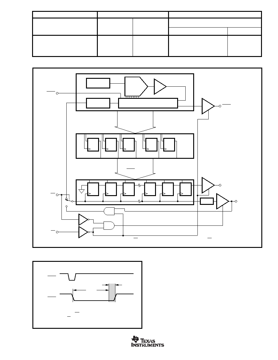
FIGURE 3. Block Diagram of the ADS7812’s Digital Inputs and Outputs.
READING DATA
The ADS7812’s digital output is in Binary Two’s Comple-
ment (BTC) format. Table III shows the relationship be-
tween the digital output word and the analog input voltage
under ideal conditions.
Figure 3 shows the relationship between the various digital
inputs, digital outputs, and internal logic of the ADS7812.
Figure 4 shows when the internal shift register of the
ADS7812 is updated and how this relates to a single conver-
sion cycle. Together, these two figures point out a very
important aspect of the ADS7812: the conversion result is
not available until after the conversion is complete. The
implications of this are discussed in the following sections.
FIGURE 4. Timing of the Shift Register Update.
Q
D
S0
Q
Update of the shift
register occurs just prior
to BUSY Rising(1)
D
S1
Q
D
S2
Q
D
S10
Q
D
S11
Q
Shift Register
Working Register
Converter Core
D
SOUT
Q
D
W0
Q
Each flip-flop in the
working register is
latched as the
conversion proceeds
D
W1
Q
D
W2
Q
D
W10
Q
D
W11
Delay
DATA
BUSY
DATACLK
CDAC
Control Logic
Clock
REF
EXT/INT
CONV
CS
NOTE: (1) If EXT/INT is HIGH (external clock), DATACLK is HIGH, and CS is LOW
during this time, the shift register will not be updated and the conversion result will be lost.
CONV
t
6 – t25
t
25
BUSY
NOTE: Update of the internal shift register occurs in the
shaded region. If EXT/INT is HIGH, then DATACLK
must be LOW or CS must be HIGH during this time.
相关PDF资料 |
PDF描述 |
|---|---|
| SY10EL12ZG | IC DRIVER LOW IMPEDANCE 8-SOIC |
| V72C48M150BF2 | CONVERTER MOD DC/DC 48V 150W |
| VI-J6V-MX-F2 | CONVERTER MOD DC/DC 5.8V 75W |
| SY10EP16VZG | IC RCVR HS DIFF 3.3/5V 8-SOIC |
| V72C48M150BF | CONVERTER MOD DC/DC 48V 150W |
相关代理商/技术参数 |
参数描述 |
|---|---|
| ADS7812UB | 功能描述:模数转换器 - ADC Low-Power Serial 12-Bit Sampling RoHS:否 制造商:Texas Instruments 通道数量:2 结构:Sigma-Delta 转换速率:125 SPs to 8 KSPs 分辨率:24 bit 输入类型:Differential 信噪比:107 dB 接口类型:SPI 工作电源电压:1.7 V to 3.6 V, 2.7 V to 5.25 V 最大工作温度:+ 85 C 安装风格:SMD/SMT 封装 / 箱体:VQFN-32 |
| ADS7812UB/1K | 功能描述:模数转换器 - ADC Low-Power Serial 12-Bit Sampling RoHS:否 制造商:Texas Instruments 通道数量:2 结构:Sigma-Delta 转换速率:125 SPs to 8 KSPs 分辨率:24 bit 输入类型:Differential 信噪比:107 dB 接口类型:SPI 工作电源电压:1.7 V to 3.6 V, 2.7 V to 5.25 V 最大工作温度:+ 85 C 安装风格:SMD/SMT 封装 / 箱体:VQFN-32 |
| ADS7812UB/1KE4 | 功能描述:模数转换器 - ADC Low-Power Serial 12-Bit Sampling RoHS:否 制造商:Texas Instruments 通道数量:2 结构:Sigma-Delta 转换速率:125 SPs to 8 KSPs 分辨率:24 bit 输入类型:Differential 信噪比:107 dB 接口类型:SPI 工作电源电压:1.7 V to 3.6 V, 2.7 V to 5.25 V 最大工作温度:+ 85 C 安装风格:SMD/SMT 封装 / 箱体:VQFN-32 |
| ADS7812UB/1KG4 | 功能描述:模数转换器 - ADC Low-Pwr Serial 12B Sampling ADC RoHS:否 制造商:Texas Instruments 通道数量:2 结构:Sigma-Delta 转换速率:125 SPs to 8 KSPs 分辨率:24 bit 输入类型:Differential 信噪比:107 dB 接口类型:SPI 工作电源电压:1.7 V to 3.6 V, 2.7 V to 5.25 V 最大工作温度:+ 85 C 安装风格:SMD/SMT 封装 / 箱体:VQFN-32 |
| ADS7812UBE4 | 功能描述:模数转换器 - ADC Low-Power Serial 12-Bit Sampling RoHS:否 制造商:Texas Instruments 通道数量:2 结构:Sigma-Delta 转换速率:125 SPs to 8 KSPs 分辨率:24 bit 输入类型:Differential 信噪比:107 dB 接口类型:SPI 工作电源电压:1.7 V to 3.6 V, 2.7 V to 5.25 V 最大工作温度:+ 85 C 安装风格:SMD/SMT 封装 / 箱体:VQFN-32 |
发布紧急采购,3分钟左右您将得到回复。