- 您现在的位置:买卖IC网 > PDF目录10467 > ADS7818E/2K5 (Texas Instruments)IC 12-BIT 500KHZ 10MW A/D 8-MSOP PDF资料下载
参数资料
| 型号: | ADS7818E/2K5 |
| 厂商: | Texas Instruments |
| 文件页数: | 21/21页 |
| 文件大小: | 0K |
| 描述: | IC 12-BIT 500KHZ 10MW A/D 8-MSOP |
| 产品培训模块: | Data Converter Basics |
| 标准包装: | 2,500 |
| 位数: | 12 |
| 采样率(每秒): | 500k |
| 数据接口: | 串行 |
| 转换器数目: | 1 |
| 功率耗散(最大): | 20mW |
| 电压电源: | 单电源 |
| 工作温度: | -40°C ~ 85°C |
| 安装类型: | 表面贴装 |
| 封装/外壳: | 8-TSSOP,8-MSOP(0.118",3.00mm 宽) |
| 供应商设备封装: | 8-MSOP |
| 包装: | 带卷 (TR) |
| 输入数目和类型: | 1 个差分,单极 |
| 配用: | 296-19913-ND - EVAL MOD FOR ADS7818 |
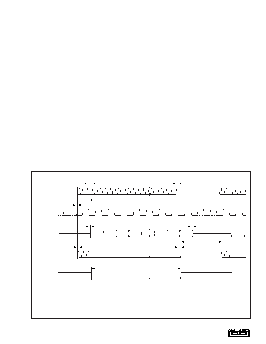
9
ADS7818
D11
(MSB)
DATA
NOTES: (1) Clock periods 14 and 15 are shown for clarity, but are not required for proper operation of the ADS7818, provided that the
minimum t
ACQ time is met. The CLK input may remain HIGH or LOW during this period. (2) The transition from sample mode to hold
mode occurs on the falling edge of CONV. This transition is not dependent on CLK. (3) The device remains fully powered when
operated as shown. If the sample time is longer than 3 clock periods, power consumption can be reduced by allowing the device to
enter a power down mode. See the power down timing for more information.
HOLD
CONVERSION IN PROGRESS
IDLE
IDLE(3)
SAMPLE
(2)
(1)
HOLD
CLK
1
2
3
4
11
12
13
14
15
14
15
16
1
CONV
SAMPLE/HOLD
MODE
INTERNAL
CONVERSION
STATE
D10
D9
D2
D1
D0
(LSB)
t
CKDE
t
CVHD
t
CONV
t
ACQ
t
CKCS
t
CKCH
t
CKSP
t
CVL
t
CKDD
t
CVCK
faster than the 10ns indicated by tCKCH, then there is a
chance that some digital feedthrough may be coupled onto
the hold capacitor. This could cause a small offset error for
that particular conversion.
Thus, there are two basic ways to operate the ADS7818.
CONV can be synchronous to CLK and CLK can be con-
tinuous. This would be the typical situation when interfacing
the converter to a digital signal processor. The second
method involves having CONV asynchronous to CLK and
gating the operation of CLK (a non-continuous clock). This
method would be more typical of an SPI-like interface on a
microcontroller. This method would also allow CONV to be
generated by a trigger circuit and to initiate (after some
delay) the start of CLK. These two methods are covered
under DSP Interfacing and SPI Interfacing.
POWER-DOWN TIMING
The conversion timing shown in Figure 3 does not result in
the ADS7818 going into the power-down mode. If the
conversion rate of the device is high (approaching 500kHz),
then there is very little power that can be saved by using the
power-down mode. However, since the power-down mode
incurs no conversion penalty (the very first conversion is
valid), at lower sample rates, significant power can be saved
by allowing the device to go into power-down mode be-
tween conversions.
Figure 4 shows the typical method for placing the A/D into
the power-down mode. If CONV is kept LOW during the
conversion and is LOW at the start of the 13 clock cycle,
then the device enters the power-down mode. It remains in
this mode until the rising edge of CONV. Note that CONV
must be HIGH for at least tACQ in order to sample the signal
properly as well as to power-up the internal nodes.
There are two different methods for clocking the ADS7818.
The first involves scaling the CLK input in relation to the
conversion rate. For example, an 8MHz input clock and the
timing shown in Figure 3 results in a 500kHz conversion
rate. Likewise, a 1.6MHz clock would result in a 100kHz
conversion rate. The second method involves keeping the
clock input as close to the maximum clock rate as possible
and starting conversions as needed. This timing is similar to
that shown in Figure 4. As an example, a 50kHz conversion
rate would require 160 clock periods per conversion instead
of the 16 clock periods used at 500kHz.
The main distinction between the two is the amount of time
that the ADS7818 remains in power down. In the first mode,
the converter only remains in power down for a small
number of clock periods (depending on how many clock
periods there are per each conversion). As the conversion
rate scales, the converter always spends the same percentage
of time in power down. Since less power is drawn by the
digital logic, there is a small decrease in power consump-
tion, but it is very slight. This effect can be seen in the
typical performance curve “Supply Current vs Sample Rate.”
FIGURE 3. Basic Conversion Timing.
相关PDF资料 |
PDF描述 |
|---|---|
| MS3100R20-23P | CONN RCPT 2POS WALL MNT W/PINS |
| VI-20H-MX | CONVERTER MOD DC/DC 52V 75W |
| PT00A-8-4S | CONN RCPT 4 POS WALL MNT W/SCKT |
| MS27473T12B8P | CONN PLUG 8POS STRAIGHT W/PINS |
| VE-JWV-MW-F1 | CONVERTER MOD DC/DC 5.8V 100W |
相关代理商/技术参数 |
参数描述 |
|---|---|
| ADS7818E2K5G4 | 制造商:TI 制造商全称:Texas Instruments 功能描述:12-Bit High Speed Low Power Sampling ANALOG-TO-DIGITAL CONVERTER |
| ADS7818EB | 制造商:BB 制造商全称:BB 功能描述:2SC5161 |
| ADS7818EB/250 | 功能描述:模数转换器 - ADC 12-Bit High Speed Low Power Sampling RoHS:否 制造商:Texas Instruments 通道数量:2 结构:Sigma-Delta 转换速率:125 SPs to 8 KSPs 分辨率:24 bit 输入类型:Differential 信噪比:107 dB 接口类型:SPI 工作电源电压:1.7 V to 3.6 V, 2.7 V to 5.25 V 最大工作温度:+ 85 C 安装风格:SMD/SMT 封装 / 箱体:VQFN-32 |
| ADS7818EB/250G4 | 功能描述:模数转换器 - ADC 12-Bit High Speed Low Power Sampling RoHS:否 制造商:Texas Instruments 通道数量:2 结构:Sigma-Delta 转换速率:125 SPs to 8 KSPs 分辨率:24 bit 输入类型:Differential 信噪比:107 dB 接口类型:SPI 工作电源电压:1.7 V to 3.6 V, 2.7 V to 5.25 V 最大工作温度:+ 85 C 安装风格:SMD/SMT 封装 / 箱体:VQFN-32 |
| ADS7818EB/2K5 | 功能描述:模数转换器 - ADC 12-Bit High Speed Low Power Sampling RoHS:否 制造商:Texas Instruments 通道数量:2 结构:Sigma-Delta 转换速率:125 SPs to 8 KSPs 分辨率:24 bit 输入类型:Differential 信噪比:107 dB 接口类型:SPI 工作电源电压:1.7 V to 3.6 V, 2.7 V to 5.25 V 最大工作温度:+ 85 C 安装风格:SMD/SMT 封装 / 箱体:VQFN-32 |
发布紧急采购,3分钟左右您将得到回复。