- 您现在的位置:买卖IC网 > PDF目录10370 > ADS7825PB (Texas Instruments)IC 16-BIT 4-CHAN MUX A/D 28-DIP PDF资料下载
参数资料
| 型号: | ADS7825PB |
| 厂商: | Texas Instruments |
| 文件页数: | 16/21页 |
| 文件大小: | 0K |
| 描述: | IC 16-BIT 4-CHAN MUX A/D 28-DIP |
| 产品培训模块: | Data Converter Basics |
| 标准包装: | 13 |
| 位数: | 16 |
| 采样率(每秒): | 40k |
| 数据接口: | 串行,并联 |
| 转换器数目: | 1 |
| 功率耗散(最大): | 50mW |
| 电压电源: | 单电源 |
| 工作温度: | -40°C ~ 85°C |
| 安装类型: | 通孔 |
| 封装/外壳: | 28-DIP(0.300",7.62mm) |
| 供应商设备封装: | 28-PDIP |
| 包装: | 管件 |
| 输入数目和类型: | 4 个单端,双极 |
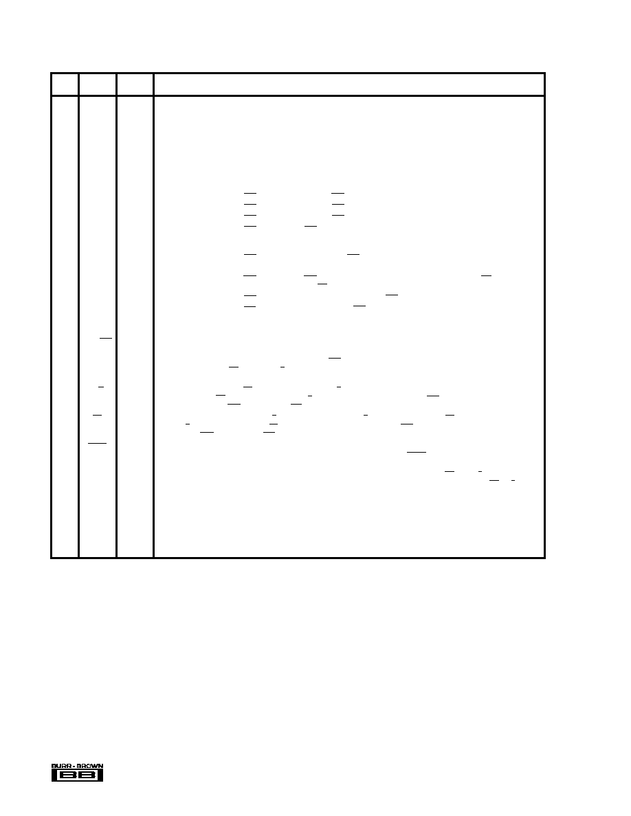
4
ADS7825
PIN #
NAME
I/O
DESCRIPTION
PIN ASSIGNMENTS
1
AGND1
Analog Ground. Used internally as ground reference point.
2
AIN0
Analog Input Channel 0. Full-scale input range is
±10V.
3
AIN1
Analog Input Channel 1. Full-scale input range is
±10V.
4
AIN2
Analog Input Channel 2. Full-scale input range is
±10V.
5
AIN3
Analog Input Channel 3. Full-scale input range is
±10V.
6
CAP
Internal Reference Output Buffer. 2.2
F Tantalum to ground.
7
REF
Reference Input/Output. Outputs +2.5V nominal. If used externally, must be buffered to maintain ADS7825 accuracy.
Can also be driven by external system reference. In both cases, bypass to ground with a 2.2
F Tantalum capacitor.
8
AGND2
Analog Ground.
9
D7
O
Parallel Data Bit 7 if PAR/SER HIGH; Tri-state if PAR/SER LOW. See Table I.
10
D6
O
Parallel Data Bit 6 if PAR/SER HIGH; Tri-state if PAR/SER LOW. See Table I.
11
D5
O
Parallel Data Bit 5 if PAR/SER HIGH; Tri-state if PAR/SER LOW. See Table I.
12
D4
I/O
Parallel Data Bit 4 if PAR/SER HIGH; if PAR/SER LOW, a LOW level input here will transmit serial data on SDATA from
the previous conversion using the internal serial clock; a HIGH input here will transmit serial data using an external serial
clock input on DATACLK (D2). See Table I.
13
D3
O
Parallel Data Bit 3 if PAR/SER HIGH; SYNC output if PAR/SER LOW. See Table I.
14
DGND
Digital Ground.
15
D2
I/O
Parallel Data Bit 2 if PAR/SER HIGH; if PAR/SER LOW, this will output the internal serial clock if EXT/INT (D4) is LOW;
will be an input for an external serial clock if EXT/INT (D4) is HIGH. See Table I.
16
D1
O
Parallel Data Bit 1 if PAR/SER HIGH; SDATA serial data output if PAR/SER LOW. See Table I.
17
D0
I/O
Parallel Data Bit 0 if PAR/SER HIGH; TAG data input if PAR/SER LOW. See Table I.
18
A1
I/O
Channel Address. Input if CONTC LOW, output if CONTC HIGH. See Table I.
19
A0
I/O
Channel Address. Input if CONTC LOW, output if CONTC HIGH. See Table I.
20
PAR/SER
I
Select Parallel or Serial Output. If HIGH, parallel data will be output on D0 thru D7. If LOW, serial data will be output on
SDATA. See Table I and Figure 1.
21
BYTE
I
Byte Select. Only used with parallel data, when PAR/SER HIGH. Determines which byte is available on D0 thru D7.
Changing BYTE with CS LOW and R/C HIGH will cause the data bus to change accordingly. LOW selects the 8 MSBs;
HIGH selects the 8 LSBs. See Figures 2 and 3
22
R/C
I
Read/Convert Input. With CS LOW, a falling edge on R/C puts the internal sample/hold into the hold state and starts a
conversion. With CS LOW, a rising edge on R/C enables the output data bits if PAR/SER HIGH, or starts transmission
of serial data if PAR/SER LOW and EXT/INT HIGH.
23
CS
I
Chip Select. Internally OR'd with R/C. With CONTC LOW and R/C LOW, a falling edge on CS will initiate a conversion.
With R/C HIGH, a falling edge on CS will enable the output data bits if PAR/SER HIGH, or starts transmission of serial
data if PAR/SER LOW and EXT/INT HIGH.
24
BUSY
O
Busy Output. Falls when conversion is started; remains LOW until the conversion is completed and the data is latched
into the output register. In parallel output mode, output data will be valid when BUSY rises, so that the rising edge
can be used to latch the data.
25
CONTC
I
Continuous Conversion Input. If LOW, conversions will occur normally when initiated using CS and R/C; if HIGH,
acquisition and conversions will take place continually, cycling through all four input channels, as long as CS, R/C and
PWRD are LOW. See Table I. For serial mode only.
26
PWRD
I
Power Down Input. If HIGH, conversions are inhibited and power consumption is significantly reduced. Results from the
previous conversion are maintained in the output register. In the continuous conversion mode, the multiplexer address
channel is reset to channel 0.
27
VS2
Supply Input. Nominally +5V. Connect directly to pin 28. Decouple to ground with 0.1
F ceramic and 10F Tantalum
capacitors.
28
VS1
Supply Input. Nominally +5V. Connect directly to pin 27.
相关PDF资料 |
PDF描述 |
|---|---|
| VI-234-MX-S | CONVERTER MOD DC/DC 48V 75W |
| ADS62P43IRGC25 | IC ADC 14B SER/PAR 80MSPS 64VQFN |
| VE-BNZ-MV-S | CONVERTER MOD DC/DC 2V 60W |
| VE-B3R-MW-S | CONVERTER MOD DC/DC 7.5V 100W |
| VE-B3N-MW-S | CONVERTER MOD DC/DC 18.5V 100W |
相关代理商/技术参数 |
参数描述 |
|---|---|
| ADS7825PBG4 | 功能描述:模数转换器 - ADC 4 Ch 16B Sampling CMOS ADC RoHS:否 制造商:Texas Instruments 通道数量:2 结构:Sigma-Delta 转换速率:125 SPs to 8 KSPs 分辨率:24 bit 输入类型:Differential 信噪比:107 dB 接口类型:SPI 工作电源电压:1.7 V to 3.6 V, 2.7 V to 5.25 V 最大工作温度:+ 85 C 安装风格:SMD/SMT 封装 / 箱体:VQFN-32 |
| ADS7825PG4 | 功能描述:模数转换器 - ADC 4 Channel 16-Bit Sampling CMOS RoHS:否 制造商:Texas Instruments 通道数量:2 结构:Sigma-Delta 转换速率:125 SPs to 8 KSPs 分辨率:24 bit 输入类型:Differential 信噪比:107 dB 接口类型:SPI 工作电源电压:1.7 V to 3.6 V, 2.7 V to 5.25 V 最大工作温度:+ 85 C 安装风格:SMD/SMT 封装 / 箱体:VQFN-32 |
| ADS7825U | 功能描述:模数转换器 - ADC 4 Channel 16-Bit Sampling CMOS RoHS:否 制造商:Texas Instruments 通道数量:2 结构:Sigma-Delta 转换速率:125 SPs to 8 KSPs 分辨率:24 bit 输入类型:Differential 信噪比:107 dB 接口类型:SPI 工作电源电压:1.7 V to 3.6 V, 2.7 V to 5.25 V 最大工作温度:+ 85 C 安装风格:SMD/SMT 封装 / 箱体:VQFN-32 |
| ADS7825U | 制造商:BURR-BROWN 功能描述:16BIT ADC 4CH SMD 7825 SOIC28 |
| ADS7825U/1K | 功能描述:模数转换器 - ADC 4 Channel 16-Bit Sampling CMOS RoHS:否 制造商:Texas Instruments 通道数量:2 结构:Sigma-Delta 转换速率:125 SPs to 8 KSPs 分辨率:24 bit 输入类型:Differential 信噪比:107 dB 接口类型:SPI 工作电源电压:1.7 V to 3.6 V, 2.7 V to 5.25 V 最大工作温度:+ 85 C 安装风格:SMD/SMT 封装 / 箱体:VQFN-32 |
发布紧急采购,3分钟左右您将得到回复。