- 您现在的位置:买卖IC网 > PDF目录10716 > ADS7864YB/250 (Texas Instruments)IC 12BIT 500KHZ 6CH A/D 48-TQFP PDF资料下载
参数资料
| 型号: | ADS7864YB/250 |
| 厂商: | Texas Instruments |
| 文件页数: | 3/27页 |
| 文件大小: | 0K |
| 描述: | IC 12BIT 500KHZ 6CH A/D 48-TQFP |
| 产品培训模块: | Data Converter Basics |
| 标准包装: | 1 |
| 位数: | 12 |
| 采样率(每秒): | 500k |
| 数据接口: | 并联 |
| 转换器数目: | 2 |
| 功率耗散(最大): | 50mW |
| 电压电源: | 模拟和数字 |
| 工作温度: | -40°C ~ 85°C |
| 安装类型: | 表面贴装 |
| 封装/外壳: | 48-TQFP |
| 供应商设备封装: | 48-TQFP(7x7) |
| 包装: | 标准包装 |
| 输入数目和类型: | 12 个单端,双极;6 个差分,双极 |
| 产品目录页面: | 892 (CN2011-ZH PDF) |
| 配用: | 296-30697-ND - EVAL MODULE FOR ADS7864M |
| 其它名称: | ADS7864YBDKR |
第1页第2页当前第3页第4页第5页第6页第7页第8页第9页第10页第11页第12页第13页第14页第15页第16页第17页第18页第19页第20页第21页第22页第23页第24页第25页第26页第27页
www.ti.com
APPLICATIONS INFORMATION
INTRODUCTION
REFERENCE
ANALOG INPUT
SAMPLE-AND-HOLD SECTION
ADS7864
SingleEnded Input
Common
Voltage
V
REF to +VREF
peaktopeak
Differential Input
Common
Voltage
V
REF
peaktopeak
V
REF
peaktopeak
ADS7864
SBAS141A – SEPTEMBER 2000 – REVISED MARCH 2005
signal, is 5ns. The average delta of repeated aperture
delay values is typically 50ps (also known as aperture
jitter). These specifications reflect the ability of the
ADS7864 to capture AC input signals accurately at
The ADS7864 is a high speed, low power, dual 12-bit
the exact same moment in time.
analog-to-digital converter (ADC) that operates from a
single +5V supply. The input channels are fully
differential with a typical common-mode rejection of
80dB. The part contains dual 2s successive approxi-
Under normal operation, the REFOUT pin (pin 2)
mation ADCs, six differential sample-and-hold ampli-
should be directly connected to the REFIN pin (pin 1)
fiers, an internal +2.5V reference with REFIN and
to provide an internal +2.5V reference to the
REFOUT pins and a high speed parallel interface.
ADS7864. The ADS7864 can operate, however, with
There are six analog inputs that are grouped into
an external reference in the range of 1.2V to 2.6V for
three channels (A, B and C). Each A/D converter has
a corresponding full-scale range of 2.4V to 5.2V.
three inputs (A0/A1, B0/B1 and C0/C1) that can be
The
internal
reference
of
the
ADS7864
is
sampled and converted simultaneously, thus pre-
double-buffered. If the internal reference is used to
serving the relative phase information of the signals
drive an external load, a buffer is provided between
on both analog inputs. Each pair of channels has a
the reference and the load applied to pin 33 (the
hold signal (HOLDA, HOLDB, HOLDC) to allow
internal reference can typically source 2mA of cur-
simultaneous sampling on all six channels. The part
rent—load capacitance should not exceed 100pF). If
accepts an analog input voltage in the range of –VREF
an external reference is used, the second buffer
to +VREF, centered around the internal +2.5V refer-
provides isolation between the external reference and
ence. The part will also accept bipolar input ranges
the CDAC. This buffer is also used to recharge all of
when a level shift circuit is used at the front end (see
the capacitors of both CDACs during conversion.
A conversion is initiated on the ADS7864 by bringing
the HOLDX pin low for a minimum of 15ns. HOLDX
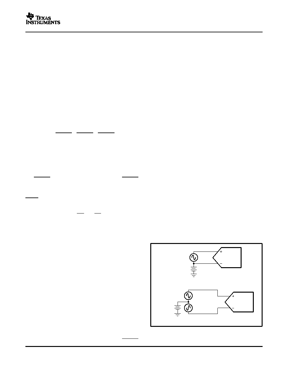
The analog input is bipolar and fully differential. There
low places both sample-and-hold amplifiers of the X
are two general methods of driving the analog input
channels in the hold state simultaneously and the
of the ADS7864: single-ended or differential (see
conversion process is started on both channels. The
Figure 19 and Figure 20). When the input is
BUSY output will then go low and remain low for the
single-ended, the –IN input is held at the com-
duration of the conversion cycle. The data can be
mon-mode voltage. The +IN input swings around the
read from the parallel output bus following the con-
same common voltage and the peak-to-peak ampli-
version by bringing both RD and CS low.
tude
is
the
(common-mode
+VREF)
and
the
Conversion time for the ADS7864 is 1.75s when an
(common-mode –VREF). The value of VREF determines
8MHz external clock is used. The corresponding
the range over which the common-mode voltage may
acquisition time is 0.25s. To achieve maximum
vary (see Figure 21).
output rate (500kHz), the read function can be
performed during at the start of the next conversion.
NOTE: This mode of operation is described in more
detail in the Timing and Control section of this data
sheet.
The sample-and-hold amplifiers on the ADS7864
allow the ADCs to accurately convert an input sine
wave of full-scale amplitude to 12-bit accuracy. The
input bandwidth of the sample-and-hold is greater
than the Nyquist rate of the ADC (Nyquist equals
one-half of the sampling rate) even when the ADC is
operated at its maximum throughput rate of 500kHz.
The
typical
small-signal
bandwidth
of
the
sample-and-hold amplifiers is 40MHz.
Typical aperture delay time, or the time it takes for
Figure 19. Methods of Driving the ADS7864
the ADS7864 to switch from the sample to the hold
Single-Ended or Differential
mode following the negative edge of the HOLDX
11
相关PDF资料 |
PDF描述 |
|---|---|
| MCP6548-I/MS | IC COMP OPENDRN 1.6V SNGL 8-MSOP |
| MCP6547T-I/MS | IC COMP OPENDRN 1.6V DUAL 8-MSOP |
| MCP6547-I/SN | IC COMP OPENDRN 1.6V DUAL 8-SOIC |
| MCP6542-I/SN | IC COMP PUSHPULL 1.6V DUAL 8SOIC |
| MCP6542-I/P | IC COMP PUSHPULL 1.6V DUAL 8-DIP |
相关代理商/技术参数 |
参数描述 |
|---|---|
| ADS7865 | 制造商:TI 制造商全称:Texas Instruments 功能描述:Dual, 12-Bit, 3+3 or 2+2 Channel, Simultaneous Sampling Analog-to-Digital Converter |
| ADS7865I | 制造商:TI 制造商全称:Texas Instruments 功能描述:Dual, 12-Bit, 3+3 or 2+2 Channel, Simultaneous Sampling Analog-to-Digital Converter |
| ADS7865IBPBSR | 制造商:TI 制造商全称:Texas Instruments 功能描述:Dual, 12-Bit, 3+3 or 2+2 Channel, Simultaneous Sampling Analog-to-Digital Converter |
| ADS7865IPBS | 功能描述:模数转换器 - ADC Dual 2MSPS 12B Simul ADC RoHS:否 制造商:Texas Instruments 通道数量:2 结构:Sigma-Delta 转换速率:125 SPs to 8 KSPs 分辨率:24 bit 输入类型:Differential 信噪比:107 dB 接口类型:SPI 工作电源电压:1.7 V to 3.6 V, 2.7 V to 5.25 V 最大工作温度:+ 85 C 安装风格:SMD/SMT 封装 / 箱体:VQFN-32 |
| ADS7865IPBSG4 | 功能描述:模数转换器 - ADC Dual,2MSPS,12B,2+2 Ch,ADC RoHS:否 制造商:Texas Instruments 通道数量:2 结构:Sigma-Delta 转换速率:125 SPs to 8 KSPs 分辨率:24 bit 输入类型:Differential 信噪比:107 dB 接口类型:SPI 工作电源电压:1.7 V to 3.6 V, 2.7 V to 5.25 V 最大工作温度:+ 85 C 安装风格:SMD/SMT 封装 / 箱体:VQFN-32 |
发布紧急采购,3分钟左右您将得到回复。