- 您现在的位置:买卖IC网 > PDF目录10411 > ADS828E/1K (Texas Instruments)IC 10BIT 75MHZ ADC 28-SSOP PDF资料下载
参数资料
| 型号: | ADS828E/1K |
| 厂商: | Texas Instruments |
| 文件页数: | 4/17页 |
| 文件大小: | 0K |
| 描述: | IC 10BIT 75MHZ ADC 28-SSOP |
| 产品培训模块: | Data Converter Basics |
| 标准包装: | 1,000 |
| 系列: | SpeedPlus™ |
| 位数: | 10 |
| 采样率(每秒): | 75M |
| 数据接口: | 并联 |
| 转换器数目: | 1 |
| 功率耗散(最大): | 340mW |
| 电压电源: | 单电源 |
| 工作温度: | -40°C ~ 85°C |
| 安装类型: | 表面贴装 |
| 封装/外壳: | 28-SSOP(0.209",5.30mm 宽) |
| 供应商设备封装: | 28-SSOP |
| 包装: | 带卷 (TR) |
| 输入数目和类型: | 2 个单端,单极;1 个差分,单极 |
ADS828
12
SBAS126A
Jitter SNR
t
rms signal to rms noise
IN
A
=
20
1
2
log π
FIGURE 9. Recommended Bypassing for the Supply Pins.
+FS –1LSB (IN = +3V, IN = +2V)
11 1111 1111
+1/2 Full Scale
11 0000 0000
Bipolar Zero (IN = IN = CMV)
10 0000 0000
–1/2 Full Scale
01 0000 0000
–FS (IN = +2V, IN = +3V)
00 0000 0000
STRAIGHT OFFSET BINARY
DIFFERENTIAL INPUT
(SOB)
TABLE II. Coding Table for Differential Input Configuration
and 2Vp-p Full-Scale Range.
+FS –1LSB (IN = REFT)
11 1111 1111
+1/2 Full Scale
11 0000 0000
Bipolar Zero (IN = CMV)
10 0000 0000
–1/2 Full Scale
01 0000 0000
–FS (IN = REFB)
00 0000 0000
SINGLE-ENDED INPUT
STRAIGHT OFFSET BINARY
(IN = CMV)
(SOB)
TABLE I. Coding Table for Single-Ended Input Configura-
tion with IN Tied to the Common-Mode Voltage
(CMV).
given by the following equation. If this value is near your
system requirements, input clock jitter must be reduced.
where: IN is input signal frequency
tA is rms clock jitter
Special consideration should be given to clock jitter, particu-
larly in undersampling applications. The clock input should
be treated as an analog input in order to achieve the highest
level of performance. Any overshoot or undershoot of the
clock signal may cause degradation of performance. When
digitizing at high sampling rates, the clock should have 50%
duty cycle (tH = tL), along with fast rise and fall times of 2ns
or less. The clock input of the ADS828 can be driven with
either 3V or 5V logic levels. Using low-voltage logic (3V)
may lead to improved AC performance of the converter.
Digital Outputs
The output data format of the ADS828 is in positive Straight
Offset Binary code, see Tables I and II. This format can
easily be converted into the Binary Two’s Complement code
by inverting the MSB.
It is recommended to keep the capacitive loading on the data
lines as low as possible (
≤ 15pF). Higher capacitive loading
will cause larger dynamic currents as the digital outputs are
changing. Those high current surges can feed back to the
analog portion of the ADS828 and affect the performance. If
necessary, external buffers or latches close to the converter’s
output pins may be used to minimize the capacitive loading.
They also provide the added benefit of isolating the ADS828
from any digital noise activities on the bus coupling back
high frequency noise.
Digital Output Driver (VDRV)
The ADS828 features a dedicated supply pin for the output
logic drivers, VDRV, which is not internally connected to
the other supply pins. By setting the voltage at VDRV to
+5V or +3V, the ADS828 produces corresponding logic
levels and can directly interface to the selected logic family.
The output stages are designed to supply sufficient current to
drive a variety of logic families. However, it is recom-
mended to use the ADS828 with +3V logic supply. This will
lower the power dissipation in the output stages due to the
lower output swing and reduce current glitches on the supply
line, which may affect the ac performance of the converter.
In some applications, it might be advantageous to decouple
the VDRV pin with additional capacitors or a pi-filter.
GROUNDING AND DECOUPLING
Proper grounding and bypassing, short lead length, and the
use of ground planes are particularly important for high
frequency designs. Multilayer PC boards are recommended
for best performance since they offer distinct advantages like
minimizing ground impedance, separation of signal layers
by ground layers, etc. The ADS828 should be treated as an
analog component. Whenever possible, the supply pins should
be powered by the analog supply. This will ensure the most
consistent results since digital supply lines often carry high
levels of noise which otherwise would be coupled into the
converter and degrade the achievable performance. All ground
connections on the ADS828 are internally joined together,
obviating the design of split ground planes. The ground pins
(1, 16, 26) should directly connect to an analog ground
plane, which covers the PC board area around the converter.
While designing the layout, it is important to keep the analog
signal traces separated from any digital lines to prevent noise
coupling onto the analog signal path. Because of its high
sampling rate the, ADS828 generates high frequency current
transients and noise (clock feedthrough) that are fed back
into the supply and reference lines. This requires that all
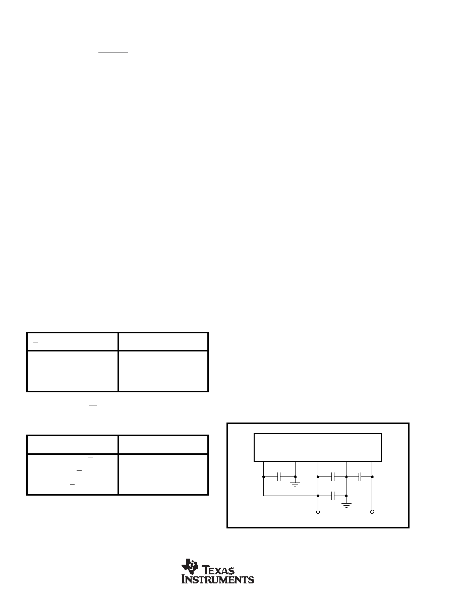
supply and reference pins be sufficiently bypassed. Figure 9
shows the recommended decoupling scheme for the ADS828.
In most cases, 0.1
F ceramic chip capacitors at each pin are
adequate to keep the impedance low over a wide frequency
range. Their effectiveness largely depends on the proximity
to the individual supply pin. Therefore, they should be
located as close to the supply pins as possible. In addition,
a larger bipolar capacitor (1
F to 22F) should be placed on
the PC board in proximity of the converter circuit.
+V
S
27
26
GND
ADS828
+
0.1
F
0.1
F
+V
S
15
16
GND
10
F
+5V
VDRV
28
0.1
F
+3/+5V
相关PDF资料 |
PDF描述 |
|---|---|
| VI-21M-IW-F3 | CONVERTER MOD DC/DC 10V 100W |
| MS3106A22-23P | CONN PLUG 8POS STRAIGHT W/PINS |
| VE-23V-IW-F4 | CONVERTER MOD DC/DC 5.8V 100W |
| VE-JWZ-MX-B1 | CONVERTER MOD DC/DC 2V 30W |
| VI-21L-IW-F3 | CONVERTER MOD DC/DC 28V 100W |
相关代理商/技术参数 |
参数描述 |
|---|---|
| ADS828EG4 | 功能描述:模数转换器 - ADC 10-Bit 75 MSPS SE/Diff Int/Ext Ref RoHS:否 制造商:Texas Instruments 通道数量:2 结构:Sigma-Delta 转换速率:125 SPs to 8 KSPs 分辨率:24 bit 输入类型:Differential 信噪比:107 dB 接口类型:SPI 工作电源电压:1.7 V to 3.6 V, 2.7 V to 5.25 V 最大工作温度:+ 85 C 安装风格:SMD/SMT 封装 / 箱体:VQFN-32 |
| ADS830 | 制造商:BB 制造商全称:BB 功能描述:8-Bit, 60MHz Sampling ANALOG-TO-DIGITAL CONVERTER |
| ADS830E | 功能描述:模数转换器 - ADC 8-Bit 60 MSPS SE/Diff Inputs RoHS:否 制造商:Texas Instruments 通道数量:2 结构:Sigma-Delta 转换速率:125 SPs to 8 KSPs 分辨率:24 bit 输入类型:Differential 信噪比:107 dB 接口类型:SPI 工作电源电压:1.7 V to 3.6 V, 2.7 V to 5.25 V 最大工作温度:+ 85 C 安装风格:SMD/SMT 封装 / 箱体:VQFN-32 |
| ADS830E/2K5 | 功能描述:模数转换器 - ADC 8-Bit 60 MSPS SE/Diff Inputs RoHS:否 制造商:Texas Instruments 通道数量:2 结构:Sigma-Delta 转换速率:125 SPs to 8 KSPs 分辨率:24 bit 输入类型:Differential 信噪比:107 dB 接口类型:SPI 工作电源电压:1.7 V to 3.6 V, 2.7 V to 5.25 V 最大工作温度:+ 85 C 安装风格:SMD/SMT 封装 / 箱体:VQFN-32 |
| ADS830E/2K5G4 | 功能描述:模数转换器 - ADC 8-Bit 60 MSPS SE/Diff Inputs RoHS:否 制造商:Texas Instruments 通道数量:2 结构:Sigma-Delta 转换速率:125 SPs to 8 KSPs 分辨率:24 bit 输入类型:Differential 信噪比:107 dB 接口类型:SPI 工作电源电压:1.7 V to 3.6 V, 2.7 V to 5.25 V 最大工作温度:+ 85 C 安装风格:SMD/SMT 封装 / 箱体:VQFN-32 |
发布紧急采购,3分钟左右您将得到回复。