- 您现在的位置:买卖IC网 > PDF目录10416 > ADS8361IRHBTG4 (Texas Instruments)IC ADC DUAL 16BIT 500KSPS 32VQFN PDF资料下载
参数资料
| 型号: | ADS8361IRHBTG4 |
| 厂商: | Texas Instruments |
| 文件页数: | 26/29页 |
| 文件大小: | 0K |
| 描述: | IC ADC DUAL 16BIT 500KSPS 32VQFN |
| 产品培训模块: | Data Converter Basics |
| 标准包装: | 250 |
| 位数: | 16 |
| 采样率(每秒): | 500k |
| 数据接口: | 串行 |
| 转换器数目: | 2 |
| 功率耗散(最大): | 200mW |
| 电压电源: | 模拟和数字 |
| 工作温度: | -40°C ~ 125°C |
| 安装类型: | 表面贴装 |
| 封装/外壳: | 32-VFQFN 裸露焊盘 |
| 供应商设备封装: | 32-QFN 裸露焊盘(5x5) |
| 包装: | 带卷 (TR) |
| 输入数目和类型: | 8 个单端,双极;4 个差分,双极 |
| 配用: | 296-19922-ND - EVAL MOD FOR ADS8361 296-18350-ND - KIT 5-6K INTERFACE BOARD |
第1页第2页第3页第4页第5页第6页第7页第8页第9页第10页第11页第12页第13页第14页第15页第16页第17页第18页第19页第20页第21页第22页第23页第24页第25页当前第26页第27页第28页第29页
ADS8361
6
SBAS230E
www.ti.com
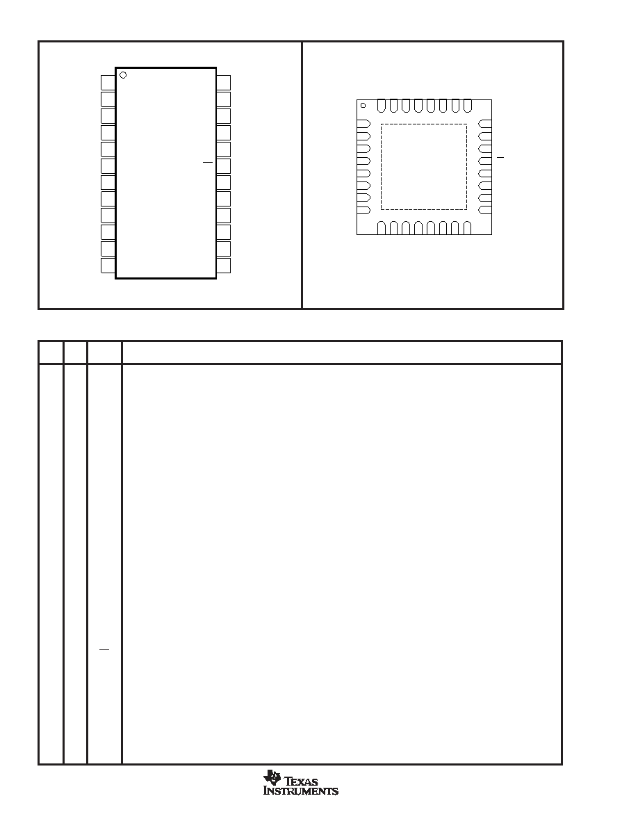
PIN CONFIGURATION
Top View
SSOP
BGND
CH B1+
CH B1–
CH B0+
CH B0–
CH A1+
CH A1–
CH A0+
CH A0–
REFIN
REFOUT
AGND
1
2
3
4
5
6
7
8
9
10
11
12
24
23
22
21
20
19
18
17
16
15
14
13
BVDD
SERIAL DATA A
SERIAL DATA B
BUSY
CLOCK
CS
RD
CONVST
A0
M0
M1
AVDD
ADS8361
Top View
QFN
SSOP QFN
PIN
NAME
DESCRIPTION
128
BGND
Digital I/O Ground. Connect directly to analog ground (pin 12).
2
1
CH B1+
Noninverting Input Channel B1
3
2
CH B1–
Inverting Input Channel B1
4
3
CH B0+
Noninverting Input Channel B0
5
4
CH B0–
Inverting Input Channel B0
6
5
CH A1+
Noninverting Input Channel A1
7
6
CH A1–
Inverting Input Channel A1
8
7
CH A0+
Noninverting Input Channel A0
9
8
CH A0–
Inverting Input Channel A0
10
9
REFIN
Reference Input
11
10
REFOUT
2.5V Reference Output
12
AGND
Analog Ground. Connect directly to digital ground (pin 1).
13
AVDD
Analog Power Supply, +5VDC. Decouple to analog ground with a 0.1μF ceramic capacitor and a 10μF tantalum capacitor.
14
16
M1
Selects between the Serial Outputs. When M1 is LOW, both Serial Output A and Serial Output B are selected for data transfer. When M1
is HIGH, Serial output A is configured for both Channel A data and Channel B data; Serial Output B goes into tri-state (i.e., high impedance).
15
17
M0
Selects between two-channel and four-channel operation. When M0 is LOW, two-channel operation is selected and operates in
conjunction with A0. When A0 is HIGH, Channel A1 and Channel B1 are being converted. When A0 is LOW, Channel A0 and Channel
B0 are being converted. When M0 is HIGH, four-channel operation is selected. In this mode, all four channels are converted in sequence
starting with Channels A0 and B0, followed by Channels A1 and B1.
16
18
A0
A0 operates in conjunction with M0. With M0 LOW and A0 HIGH, Channel A1 and Channel B1 are converted. With M0 LOW and A0 LOW,
Channel A0 and Channel B0 are converted.
17
19
CONVST Convert Start. When CONVST switches from LOW to HIGH, the device switches from the sample to hold mode, independent of the status
of the external clock.
18
20
RD
Synchronization Pulse for the Serial Output.
19
21
CS
Chip Select. When LOW, the Serial Output A and Serial Output B outputs are active; when HIGH, the serial outputs are tri-stated.
20
22
CLOCK
An external CMOS-compatible clock can be applied to the CLOCK input to synchronize the conversion process to an external source.
The CLOCK pin controls the sampling rate by the equation: fSAMPLE (max) = CLOCK/20.
21
23
BUSY
BUSY goes HIGH during a conversion and returns LOW after the third LSB has been transmitted on either the Serial A or Serial B output
pin.
22
24
SERIAL
The Serial Output data word is comprised of channel information and 16 bits of data. In operation, data is valid on the falling edge of
DCLOCK for 20 edges after the rising edge of RD.
23
25
SERIAL
The Serial Output data word is comprised of channel information and 16 bits of data. In operation, data is valid on the falling edge of
DCLOCK for 20 edges after the rising edge of RD. When M1 is HIGH, both Channel A data and Channel B data are available.
24
27
BVDD
Digital I/O Power Supply, 2.7V to 5.5V
PIN DESCRIPTIONS
DATA B
DATA A
CH B1+
CH B1
CH B0+
CH B0
CH A1+
CH A1
CH A0+
CH A0
SERIAL DATA B
BUSY
CLOCK
CS
RD
CONVST
A0
M0
1
2
3
4
5
6
7
8
24
23
22
21
20
19
18
17
ADS8361(1)
NC
(2)
NC
(2)
NC
(2)
NC
(2)
BGND
BVDD
NC
(2)
SERIAL
DATA
A
32
31
30
29
28
27
26
25
REF
IN
REF
OUT
NC
(2)
AGND
AV
DD
NC
(2)
NC
(2)
M1
9
10
11
12
13
14
15
16
NOTE: (1) The thermal pad is internally connected to the substrate.
This pad can be connected to the analog ground or left floating.
Keep the thermal pad separate from the digital ground, if possible.
(2) NC = Not Connected.
相关PDF资料 |
PDF描述 |
|---|---|
| VE-B22-MX-F4 | CONVERTER MOD DC/DC 15V 75W |
| VE-B21-MX-F3 | CONVERTER MOD DC/DC 12V 75W |
| VE-26X-IU | CONVERTER MOD DC/DC 5.2V 200W |
| VI-JNF-MX | CONVERTER MOD DC/DC 72V 75W |
| SN75115DRG4 | IC DUAL DIFF DRIVER 16-SOIC |
相关代理商/技术参数 |
参数描述 |
|---|---|
| ADS8363 | 制造商:TI 制造商全称:Texas Instruments 功能描述:Dual, 1MSPS, 16-/14-/12-Bit, 4x2 or 2x2 Channel, Simultaneous Sampling Analog-to-Digital Converter |
| ADS8363EVM | 功能描述:数据转换 IC 开发工具 ADS8363 Eval Mod RoHS:否 制造商:Texas Instruments 产品:Demonstration Kits 类型:ADC 工具用于评估:ADS130E08 接口类型:SPI 工作电源电压:- 6 V to + 6 V |
| ADS8363SRHBR | 功能描述:模数转换器 - ADC 16B 1MSPS 4x2/2x2 Simu Sampling SAR RoHS:否 制造商:Texas Instruments 通道数量:2 结构:Sigma-Delta 转换速率:125 SPs to 8 KSPs 分辨率:24 bit 输入类型:Differential 信噪比:107 dB 接口类型:SPI 工作电源电压:1.7 V to 3.6 V, 2.7 V to 5.25 V 最大工作温度:+ 85 C 安装风格:SMD/SMT 封装 / 箱体:VQFN-32 |
| ADS8363SRHBT | 功能描述:模数转换器 - ADC 16B 1MSPS 4x2/2x2 Simu Sampling SAR RoHS:否 制造商:Texas Instruments 通道数量:2 结构:Sigma-Delta 转换速率:125 SPs to 8 KSPs 分辨率:24 bit 输入类型:Differential 信噪比:107 dB 接口类型:SPI 工作电源电压:1.7 V to 3.6 V, 2.7 V to 5.25 V 最大工作温度:+ 85 C 安装风格:SMD/SMT 封装 / 箱体:VQFN-32 |
| ADS8364 | 制造商:TI 制造商全称:Texas Instruments 功能描述:250kHz, 16-Bit, 6-Channel Simultaneous Sampling ANALOG-TO-DIGITAL CONVERTERS |
发布紧急采购,3分钟左右您将得到回复。