- 您现在的位置:买卖IC网 > PDF目录19503 > ADSP-2101BPZ-100 (Analog Devices Inc)IC DSP SLG 16BIT 25MHZ 68-PLCC PDF资料下载
参数资料
| 型号: | ADSP-2101BPZ-100 |
| 厂商: | Analog Devices Inc |
| 文件页数: | 14/64页 |
| 文件大小: | 0K |
| 描述: | IC DSP SLG 16BIT 25MHZ 68-PLCC |
| 标准包装: | 1 |
| 系列: | ADSP-21xx |
| 类型: | 定点 |
| 接口: | 同步串行端口(SSP) |
| 时钟速率: | 25MHz |
| 非易失内存: | 外部 |
| 芯片上RAM: | 6kB |
| 电压 - 输入/输出: | 5.00V |
| 电压 - 核心: | 5.00V |
| 工作温度: | -40°C ~ 85°C |
| 安装类型: | 表面贴装 |
| 封装/外壳: | 68-LCC(J 形引线) |
| 供应商设备封装: | 68-PLCC(24.23x24.23) |
| 包装: | 管件 |
| 产品目录页面: | 738 (CN2011-ZH PDF) |
第1页第2页第3页第4页第5页第6页第7页第8页第9页第10页第11页第12页第13页当前第14页第15页第16页第17页第18页第19页第20页第21页第22页第23页第24页第25页第26页第27页第28页第29页第30页第31页第32页第33页第34页第35页第36页第37页第38页第39页第40页第41页第42页第43页第44页第45页第46页第47页第48页第49页第50页第51页第52页第53页第54页第55页第56页第57页第58页第59页第60页第61页第62页第63页第64页
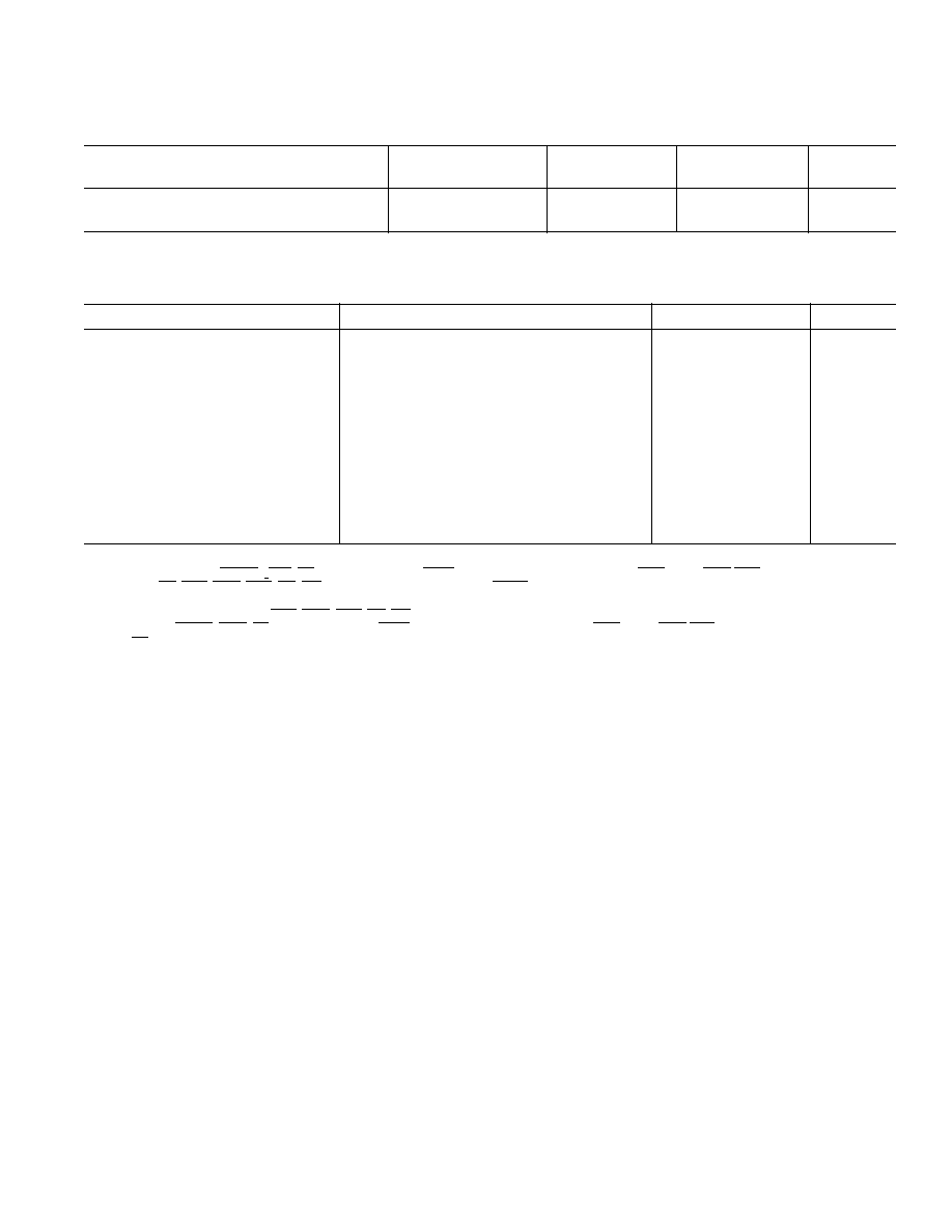
ADSP-2111–SPECIFICATIONS
RECOMMENDED OPERATING CONDITIONS
K Grade
B Grade
T Grade
Parameter
Min
Max
Min
Max
Min
Max
Unit
VDD
Supply Voltage
4.50
5.50
4.50
5.50
4.50
5.50
V
TAMB
Ambient Operating Temperature
0
+70
–40
+85
–55
+125
°C
See “Environmental Conditions” for information on thermal specifications.
ELECTRICAL CHARACTERISTICS
Parameter
Test Conditions
Min
Max
Unit
VIH
Hi-Level Input Voltage
3, 5
@ VDD = max
2.0
V
VIH
Hi-Level CLKIN Voltage
@ VDD = max
2.2
V
VIL
Lo-Level Input Voltage
1, 3
@ VDD = min
0.8
V
VOH
Hi-Level Output Voltage
2, 3, 7
@ VDD = min, IOH = –0.5 mA
2.4
V
@ VDD = min, IOH = –100
A8
VDD – 0.3
V
VOL
Lo-Level Output Voltage
2, 3, 7
@ VDD = min, IOL = 2 mA
0.4
V
IIH
Hi-Level Input Current
1
@ VDD = max, VIN = VDD max
10
A
IIL
Lo-Level Input Current
1
@ VDD = max, VIN = 0V
10
A
IOZH
Tristate Leakage Curren
4
@ VDD = max, VIN = VDD max
6
10
A
IOZL
Tristate Leakage Current
4
@ VDD = max, VIN = 0V
6
10
A
CI
Input Pin Capacitance
1, 8, 9
@ VIN = 2.5 V, fIN = 1.0 MHz, TAMB = 25
°C8
pF
CO
Output Pin Capacitance
4, 8, 9, 10
@ VIN = 2.5 V, fIN = 1.0 MHz, TAMB = 25
°C8
pF
NOTES
1Input-only pins: CLKIN, RESET, IRQ2, BR, MMAP, DR1, DR0, HSEL, HSIZE, BMODE, HMD0, HMD1, HRD/HRW, HWR/HDS, HA2/ALE, HA1-0.
2Output pins: BG, PMS, DMS, BMS, RD, WR, A0–A13, CLKOUT, DT1, DT0, HACK, FL2-0.
3Bidirectional pins: D0–D23, SCLK1, RFS1, TFS1, SCLK0, RFS0, TFS0, HD0–HD15/HAD0–HAD15.
4Tristatable pins: A0–A13, D0–D23, PMS, DMS, BMS, RD, WR, DT1, SCLK1, RSF1, TFS1, DT0, SCLK0, RFS0, TFS0, HD0–HD15/HAD0–HAD15.
5Input-only pins: RESET, IRQ2, BR, MMAP, DR1, DR0, HSEL, HSIZE, BMODE, HMD0, HMD1, HRD/HRW, HWR/HDS, HA2/ALE, HA1-0.
6 0 V on BR, CLKIN Active (to force tristate condition).
7Although specified for TTL outputs, all ADSP-2111 outputs are CMOS-compatible and will drive to V
DD and GND, assuming no dc loads.
8Guaranteed but not tested.
9Applies to ADSP-2111 PGA and PQFP packages.
10Output pin capacitance is the capacitive load for any three-stated output pin.
Specifications subject to change without notice.
ABSOLUTE MAXIMUM RATINGS*
Supply Voltage . . . . . . . . . . . . . . . . . . . . . . . . . . –0.3 V to +7 V
Input Voltage . . . . . . . . . . . . . . . . . . . . . –0.3 V to V
DD + 0.3 V
Output Voltage Swing . . . . . . . . . . . . . . –0.3 V to V
DD + 0.3 V
Operating Temperature Range (Ambient) . . . –55C to +125C
Storage Temperature Range . . . . . . . . . . . . . –65C to +150C
Lead Temperature (10 sec) PGA . . . . . . . . . . . . . . . . . +300C
Lead Temperature (5 sec) PQFP . . . . . . . . . . . . . . . . . +280C
*Stresses greater than those listed above may cause permanent damage to the
device. These are stress ratings only, and functional operation of the device at these
or any other conditions greater than those indicated in the operational sections of
this specification is not implied. Exposure to absolute maximum rating conditions
for extended periods may affect device reliability.
ADSP-21xx
REV. B
–21–
相关PDF资料 |
PDF描述 |
|---|---|
| ADSP-BF535PKBZ-300 | IC DSP CONTROLLER 16BIT 260 BGA |
| GCM15DCTN-S288 | CONN EDGECARD 30POS .156 EXTEND |
| V300A36E400BL3 | CONVERTER MOD DC/DC 36V 400W |
| KRM55WR71H226MH01K | CAP CER 22UF 50V 20% X7R 2220 |
| VE-B10-CX-B1 | CONVERTER MOD DC/DC 5V 75W |
相关代理商/技术参数 |
参数描述 |
|---|---|
| ADSP-2101BPZ-100 | 制造商:Analog Devices 功能描述:IC 16-BIT MICROCOMPUTER |
| ADSP-2101BS-100 | 制造商:Analog Devices 功能描述:DSP Fixed-Point 16-Bit 25MHz 25MIPS 80-Pin PQFP 制造商:Analog Devices 功能描述:IC MICROCOMPUTER 16-BIT |
| ADSP-2101BS-40 | 制造商:Rochester Electronics LLC 功能描述:- Bulk |
| ADSP-2101BS-50 | 制造商:Rochester Electronics LLC 功能描述:- Bulk |
| ADSP-2101BS-66 | 制造商:AD 制造商全称:Analog Devices 功能描述:ADSP-2100 Family DSP Microcomputers |
发布紧急采购,3分钟左右您将得到回复。