- 您现在的位置:买卖IC网 > PDF目录19398 > ADSP-BF504BCPZ-3F (Analog Devices Inc)IC CCD SIGNAL PROCESSOR 88LFCSP PDF资料下载
参数资料
| 型号: | ADSP-BF504BCPZ-3F |
| 厂商: | Analog Devices Inc |
| 文件页数: | 7/80页 |
| 文件大小: | 0K |
| 描述: | IC CCD SIGNAL PROCESSOR 88LFCSP |
| 视频文件: | Blackfin? BF50x Processor Family |
| 标准包装: | 1 |
| 系列: | Blackfin® |
| 类型: | 定点 |
| 接口: | CAN,EBI/EMI,I²C,IrDA,PPI,SPI,SPORT,UART/USART |
| 时钟速率: | 300MHz |
| 非易失内存: | 闪存(16MB) |
| 芯片上RAM: | 68kB |
| 电压 - 输入/输出: | 3.30V |
| 电压 - 核心: | 1.29V |
| 工作温度: | -40°C ~ 85°C |
| 安装类型: | 表面贴装 |
| 封装/外壳: | 88-VFQFN 裸露焊盘,CSP |
| 供应商设备封装: | 88-LFCSP(12x12) |
| 包装: | 托盘 |
第1页第2页第3页第4页第5页第6页当前第7页第8页第9页第10页第11页第12页第13页第14页第15页第16页第17页第18页第19页第20页第21页第22页第23页第24页第25页第26页第27页第28页第29页第30页第31页第32页第33页第34页第35页第36页第37页第38页第39页第40页第41页第42页第43页第44页第45页第46页第47页第48页第49页第50页第51页第52页第53页第54页第55页第56页第57页第58页第59页第60页第61页第62页第63页第64页第65页第66页第67页第68页第69页第70页第71页第72页第73页第74页第75页第76页第77页第78页第79页第80页
Rev. A
|
Page 15 of 80
|
July 2011
ADSP-BF504/ADSP-BF504F/ADSP-BF506F
where the variables in the equations are:
fCCLKNOM is the nominal core clock frequency
fCCLKRED is the reduced core clock frequency
VDDINTNOM is the nominal internal supply voltage
VDDINTRED is the reduced internal supply voltage
TNOM is the duration running at fCCLKNOM
TRED is the duration running at fCCLKRED
ADSP-BF50x VOLTAGE REGULATION
The ADSP-BF50x processors require an external voltage regula-
tor to power the VDDINT domain. To reduce standby power
consumption, the external voltage regulator can be signaled
through EXT_WAKE to remove power from the processor core.
This signal is high-true for power-up and may be connected
directly to the low-true shut-down input of many common
regulators.
While in the hibernate state, all external supplies (VDDEXT,
VDDFLASH) can still be applied, eliminating the need for external
buffers. The external voltage regulator can be activated from
this power down state by asserting the RESET pin, which then
initiates a boot sequence. EXT_WAKE indicates a wakeup to
the external voltage regulator.
The power good (PG) input signal allows the processor to start
only after the internal voltage has reached a chosen level. In this
way, the startup time of the external regulator is detected after
hibernation. For a complete description of the power good
functionality, refer to the ADSP-BF50x Blackfin Processor Hard-
ware Reference.
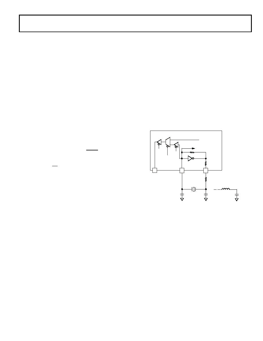
CLOCK SIGNALS
The processor can be clocked by an external crystal, a sine wave
input, or a buffered, shaped clock derived from an external
clock oscillator.
If an external clock is used, it should be a TTL-compatible signal
and must not be halted, changed, or operated below the speci-
fied frequency during normal operation. This signal is
connected to the processor’s CLKIN pin. When an external
clock is used, the XTAL pin must be left unconnected.
Alternatively, because the processor includes an on-chip oscilla-
tor circuit, an external crystal may be used. For fundamental
frequency operation, use the circuit shown in Figure 4. A paral-
lel-resonant, fundamental frequency, microprocessor-grade
crystal is connected across the CLKIN and XTAL pins. The on-
chip resistance between CLKIN and the XTAL pin is in the
500 k
Ω range. Further parallel resistors are typically not recom-
mended. The two capacitors and the series resistor shown in
Figure 4 fine tune phase and amplitude of the sine frequency.
The capacitor and resistor values shown in Figure 4 are typical
values only. The capacitor values are dependent upon the crystal
manufacturers’ load capacitance recommendations and the PCB
physical layout. The resistor value depends on the drive level
specified by the crystal manufacturer. The user should verify the
customized values based on careful investigations on multiple
devices over temperature range.
A third-overtone crystal can be used for frequencies above 25
MHz. The circuit is then modified to ensure crystal operation
only at the third overtone by adding a tuned inductor circuit as
shown in Figure 4. A design procedure for third-overtone oper-
ation is discussed in detail in (EE-168) Using Third Overtone
Crystals with the ADSP-218x DSP on the Analog Devices web-
site (www.analog.com)—use site search on “EE-168.”
The Blackfin core runs at a different clock rate than the on-chip
peripherals. As shown in Figure 5, the core clock (CCLK) and
system peripheral clock (SCLK) are derived from the input
clock (CLKIN) signal. An on-chip PLL is capable of multiplying
the CLKIN signal by a programmable multiplication factor
(bounded by specified minimum and maximum VCO frequen-
cies). The default multiplier is 6×, but it can be modified by a
software instruction sequence.
On-the-fly frequency changes can be effected by simply writing
to the PLL_DIV register. The maximum allowed CCLK and
SCLK rates depend on the applied voltages VDDINT and VDDEXT;
the VCO is always permitted to run up to the CCLK frequency
specified by the part’s speed grade. The EXTCLK pin can be
configured to output either the SCLK frequency or the input
buffered CLKIN frequency, called CLKBUF. When configured
to output SCLK (CLKOUT), the EXTCLK pin acts as a refer-
ence signal in many timing specifications. While active by
default, it can be disabled using the EBIU_AMGCTL register.
% Power Savings
1
Power Savings Factor
–
() 100%
×
=
Figure 4. External Crystal Connections
CLKIN
CLKOUT (SCLK)
XTAL
SELECT
CLKBUF
TO PLL CIRCUITRY
FOR OVERTONE
OPERATION ONLY:
NOTE: VALUES MARKED WITH * MUST BE CUSTOMIZED, DEPENDING
ON THE CRYSTAL AND LAYOUT. PLEASE ANALYZE CAREFULLY. FOR
FREQUENCIES ABOVE 33 MHz, THE SUGGESTED CAPACITOR VALUE
OF 18 pF SHOULD BE TREATED AS A MAXIMUM, AND THE SUGGESTED
RESISTOR VALUE SHOULD BE REDUCED TO 0
.
18 pF *
EN
18 pF *
330
*
Blackfin Processor
560
EXTCLK
EN
相关PDF资料 |
PDF描述 |
|---|---|
| ABC49DRTN | CONN EDGECARD 98POS .100 DIP SLD |
| TAP476M010BRW | CAP TANT 47UF 10V 20% RADIAL |
| VI-JNB-IZ | CONVERTER MOD DC/DC 95V 25W |
| MAX6514UKP055+T | IC TEMP SWITCH SOT23-5 |
| VI-J6P-IZ | CONVERTER MOD DC/DC 13.8V 25W |
相关代理商/技术参数 |
参数描述 |
|---|---|
| ADSP-BF504BCPZ-4 | 功能描述:IC CCD SIGNAL PROCESSOR 88LFCSP RoHS:是 类别:集成电路 (IC) >> 嵌入式 - DSP(数字式信号处理器) 系列:Blackfin® 标准包装:40 系列:TMS320DM64x, DaVinci™ 类型:定点 接口:I²C,McASP,McBSP 时钟速率:400MHz 非易失内存:外部 芯片上RAM:160kB 电压 - 输入/输出:3.30V 电压 - 核心:1.20V 工作温度:0°C ~ 90°C 安装类型:表面贴装 封装/外壳:548-BBGA,FCBGA 供应商设备封装:548-FCBGA(27x27) 包装:托盘 配用:TMDSDMK642-0E-ND - DEVELPER KIT W/NTSC CAMERA296-23038-ND - DSP STARTER KIT FOR TMS320C6416296-23059-ND - FLASHBURN PORTING KIT296-23058-ND - EVAL MODULE FOR DM642TMDSDMK642-ND - DEVELOPER KIT W/NTSC CAMERA |
| ADSP-BF504BCPZ-4F | 功能描述:IC CCD SIGNAL PROCESSOR 88LFCSP RoHS:是 类别:集成电路 (IC) >> 嵌入式 - DSP(数字式信号处理器) 系列:Blackfin® 标准包装:2 系列:StarCore 类型:SC140 内核 接口:DSI,以太网,RS-232 时钟速率:400MHz 非易失内存:外部 芯片上RAM:1.436MB 电压 - 输入/输出:3.30V 电压 - 核心:1.20V 工作温度:-40°C ~ 105°C 安装类型:表面贴装 封装/外壳:431-BFBGA,FCBGA 供应商设备封装:431-FCPBGA(20x20) 包装:托盘 |
| ADSP-BF504KCPZ-3F | 功能描述:IC CCD SIGNAL PROCESSOR 88LFCSP RoHS:是 类别:集成电路 (IC) >> 嵌入式 - DSP(数字式信号处理器) 系列:Blackfin® 标准包装:2 系列:StarCore 类型:SC140 内核 接口:DSI,以太网,RS-232 时钟速率:400MHz 非易失内存:外部 芯片上RAM:1.436MB 电压 - 输入/输出:3.30V 电压 - 核心:1.20V 工作温度:-40°C ~ 105°C 安装类型:表面贴装 封装/外壳:431-BFBGA,FCBGA 供应商设备封装:431-FCPBGA(20x20) 包装:托盘 |
| ADSP-BF504KCPZ-4 | 功能描述:IC CCD SIGNAL PROCESSOR 88LFCSP RoHS:是 类别:集成电路 (IC) >> 嵌入式 - DSP(数字式信号处理器) 系列:Blackfin® 标准包装:2 系列:StarCore 类型:SC140 内核 接口:DSI,以太网,RS-232 时钟速率:400MHz 非易失内存:外部 芯片上RAM:1.436MB 电压 - 输入/输出:3.30V 电压 - 核心:1.20V 工作温度:-40°C ~ 105°C 安装类型:表面贴装 封装/外壳:431-BFBGA,FCBGA 供应商设备封装:431-FCPBGA(20x20) 包装:托盘 |
| ADSP-BF504KCPZ-4F | 功能描述:IC CCD SIGNAL PROCESSOR 88LFCSP RoHS:是 类别:集成电路 (IC) >> 嵌入式 - DSP(数字式信号处理器) 系列:Blackfin® 标准包装:2 系列:StarCore 类型:SC140 内核 接口:DSI,以太网,RS-232 时钟速率:400MHz 非易失内存:外部 芯片上RAM:1.436MB 电压 - 输入/输出:3.30V 电压 - 核心:1.20V 工作温度:-40°C ~ 105°C 安装类型:表面贴装 封装/外壳:431-BFBGA,FCBGA 供应商设备封装:431-FCPBGA(20x20) 包装:托盘 |
发布紧急采购,3分钟左右您将得到回复。