- 您现在的位置:买卖IC网 > PDF目录19388 > ADSP-BF523KBCZ-6C2 (Analog Devices Inc)IC DSP CTRLR 24B W/CODEC 289BGA PDF资料下载
参数资料
| 型号: | ADSP-BF523KBCZ-6C2 |
| 厂商: | Analog Devices Inc |
| 文件页数: | 5/88页 |
| 文件大小: | 0K |
| 描述: | IC DSP CTRLR 24B W/CODEC 289BGA |
| 产品变化通告: | Datasheet Specification Change 14/Dec/2009 |
| 标准包装: | 1 |
| 系列: | Blackfin® |
| 类型: | 定点 |
| 接口: | DMA,I²C,PPI,SPI,SPORT,UART |
| 时钟速率: | 600MHz |
| 非易失内存: | ROM(32 kB) |
| 芯片上RAM: | 132kB |
| 电压 - 输入/输出: | 1.8V,2.5V,3.3V |
| 电压 - 核心: | 1.10V |
| 工作温度: | 0°C ~ 70°C |
| 安装类型: | 表面贴装 |
| 封装/外壳: | 289-LFBGA,CSPBGA |
| 供应商设备封装: | 289-CSPBGA(12x12) |
| 包装: | 托盘 |
第1页第2页第3页第4页当前第5页第6页第7页第8页第9页第10页第11页第12页第13页第14页第15页第16页第17页第18页第19页第20页第21页第22页第23页第24页第25页第26页第27页第28页第29页第30页第31页第32页第33页第34页第35页第36页第37页第38页第39页第40页第41页第42页第43页第44页第45页第46页第47页第48页第49页第50页第51页第52页第53页第54页第55页第56页第57页第58页第59页第60页第61页第62页第63页第64页第65页第66页第67页第68页第69页第70页第71页第72页第73页第74页第75页第76页第77页第78页第79页第80页第81页第82页第83页第84页第85页第86页第87页第88页
�� �
�
�ADSP-BF522/ADSP-BF523/ADSP-BF524/ADSP-BF525/ADSP-BF526/ADSP-BF527�
�length,� and� base� registers� (for� circular� buffering),� and� eight�
�additional� 32-bit� pointer� registers� (for� C-style� indexed� stack�
�manipulation).�
�Blackfin� processors� support� a� modified� Harvard� architecture� in�
�combination� with� a� hierarchical� memory� structure.� Level� 1� (L1)�
�memories� are� those� that� typically� operate� at� the� full� processor�
�speed� with� little� or� no� latency.� At� the� L1� level,� the� instruction�
�memory� holds� instructions� only.� The� two� data� memories� hold�
�data,� and� a� dedicated� scratchpad� data� memory� stores� stack� and�
�local� variable� information.�
�In� addition,� multiple� L1� memory� blocks� are� provided,� offering� a�
�configurable� mix� of� SRAM� and� cache.� The� memory� manage-�
�ment� unit� (MMU)� provides� memory� protection� for� individual�
�tasks� that� may� be� operating� on� the� core� and� can� protect� system�
�registers� from� unintended� access.�
�The� architecture� provides� three� modes� of� operation:� user� mode,�
�supervisor� mode,� and� emulation� mode.� User� mode� has�
�restricted� access� to� certain� system� resources,� thus� providing� a�
�protected� software� environment,� while� supervisor� mode� has�
�unrestricted� access� to� the� system� and� core� resources.�
�The� Blackfin� processor� instruction� set� has� been� optimized� so�
�that� 16-bit� opcodes� represent� the� most� frequently� used� instruc-�
�tions,� resulting� in� excellent� compiled� code� density.� Complex�
�DSP� instructions� are� encoded� into� 32-bit� opcodes,� representing�
�fully� featured� multifunction� instructions.� Blackfin� processors�
�support� a� limited� multi-issue� capability,� where� a� 32-bit� instruc-�
�tion� can� be� issued� in� parallel� with� two� 16-bit� instructions,�
�allowing� the� programmer� to� use� many� of� the� core� resources� in� a�
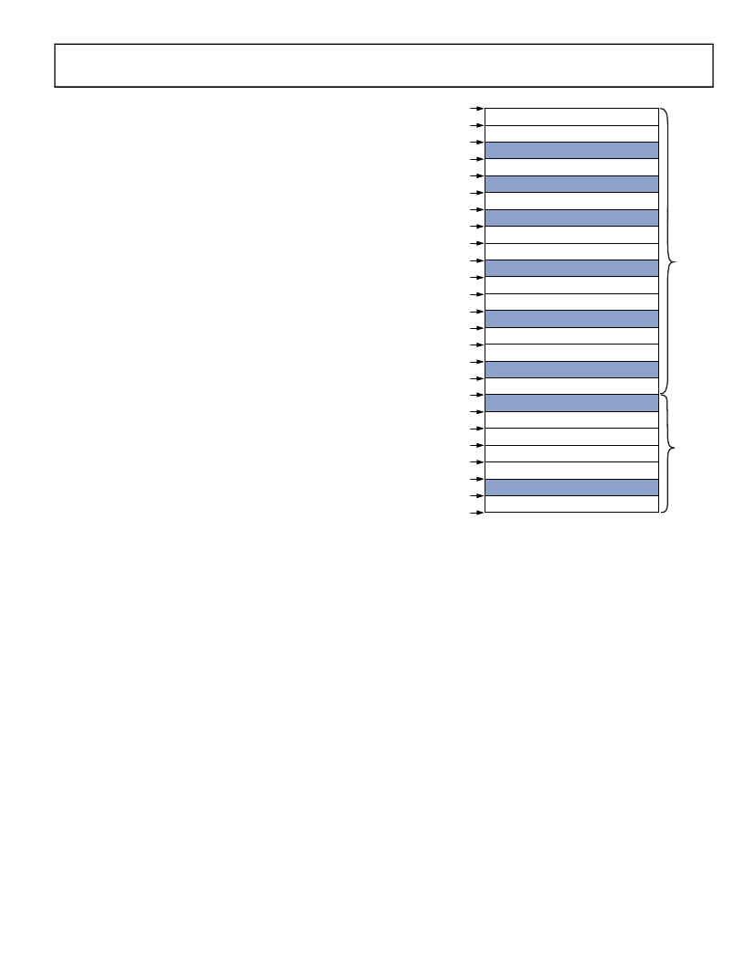
�0xFFFF� FFFF�
�0xFFE0� 0000�
�0xFFC0� 0000�
�0xFFB0� 1000�
�0xFFB0� 0000�
�0xFFA1� 4000�
�0xFFA1� 0000�
�0xFFA0� C000�
�0xFFA0� 8000�
�0xFFA0� 0000�
�0xFF90� 8000�
�0xFF90� 4000�
�0xFF90� 0000�
�0xFF80� 8000�
�0xFF80� 4000�
�0xFF80� 0000�
�0xEF00� 8000�
�0xEF00� 0000�
�0x2040� 0000�
�0x2030� 0000�
�0x2020� 0000�
�0x2010� 0000�
�0x2000� 0000�
�CORE� MMR� REGISTERS� (2M� BYTES)�
�SYSTEM� MMR� REGISTERS� (2M� BYTES)�
�RESERVED�
�SCRATCHPAD� SRAM� (4K� BYTES)�
�RESERVED�
�INSTRUCTION� SRAM� /� CACHE� (16K� BYTES)�
�RESERVED�
�INSTRUCTION� BANK� B� SRAM� (16K� BYTES)�
�INSTRUCTION� BANK� A� SRAM� (32K� BYTES)�
�RESERVED�
�DATA� BANK� B� SRAM� /� CACHE� (16K� BYTES)�
�DATA� BANK� B� SRAM� (16K� BYTES)�
�RESERVED�
�DATA� BANK� A� SRAM� /� CACHE� (16K� BYTES)�
�DATA� BANK� A� SRAM� (16K� BYTES)�
�RESERVED�
�BOOT� ROM� (32K� BYTES)�
�RESERVED�
�ASYNC� MEMORY� BANK� 3� (1M� BYTES)�
�ASYNC� MEMORY� BANK� 2� (1M� BYTES)�
�ASYNC� MEMORY� BANK� 1� (1M� BYTES)�
�ASYNC� MEMORY� BANK� 0� (1M� BYTES)�
�RESERVED�
�single� instruction� cycle.�
�0x08� 00� 0000�
�SDRAM� MEMORY� (16M� BYTES�
�128M� BYTES)�
�The� Blackfin� processor� assembly� language� uses� an� algebraic� syn-�
�tax� for� ease� of� coding� and� readability.� The� architecture� has� been�
�optimized� for� use� in� conjunction� with� the� C/C++� compiler,�
�resulting� in� fast� and� efficient� software� implementations.�
�MEMORY� ARCHITECTURE�
�The� Blackfin� processor� views� memory� as� a� single� unified�
�4G� byte� address� space,� using� 32-bit� addresses.� All� resources,�
�including� internal� memory,� external� memory,� and� I/O� control�
�registers,� occupy� separate� sections� of� this� common� address�
�space.� The� memory� portions� of� this� address� space� are� arranged�
�in� a� hierarchical� structure� to� provide� a� good� cost/performance�
�balance� of� some� very� fast,� low-latency� on-chip� memory� as� cache�
�or� SRAM,� and� larger,� lower-cost� and� performance� off-chip�
��The� on-chip� L1� memory� system� is� the� highest-performance�
�memory� available� to� the� Blackfin� processor.� The� off-chip�
�memory� system,� accessed� through� the� external� bus� interface�
�unit� (EBIU),� provides� expansion� with� SDRAM,� flash� memory,�
�and� SRAM,� optionally� accessing� up� to� 132M� bytes� of�
�physical� memory.�
�The� memory� DMA� controller� provides� high-bandwidth� data-�
�movement� capability.� It� can� perform� block� transfers� of� code�
�or� data� between� the� internal� memory� and� the� external�
�memory� spaces.�
�0x0000� 0000�
�Figure� 3.� Internal/External� Memory� Map�
�Internal� (On-Chip)� Memory�
�The� processor� has� three� blocks� of� on-chip� memory� providing�
�high-bandwidth� access� to� the� core.�
�The� first� block� is� the� L1� instruction� memory,� consisting� of�
�64K� bytes� SRAM,� of� which� 16K� bytes� can� be� configured� as� a�
�four-way� set-associative� cache.� This� memory� is� accessed� at� full�
�processor� speed.�
�The� second� on-chip� memory� block� is� the� L1� data� memory,� con-�
�sisting� of� up� to� two� banks� of� up� to� 32K� bytes� each.� Each� memory�
�bank� is� configurable,� offering� both� cache� and� SRAM� functional-�
�ity.� This� memory� block� is� accessed� at� full� processor� speed.�
�The� third� memory� block� is� a� 4K� byte� scratchpad� SRAM� which�
�runs� at� the� same� speed� as� the� L1� memories,� but� is� only� accessible�
�as� data� SRAM� and� cannot� be� configured� as� cache� memory.�
�External� (Off-Chip)� Memory�
�External� memory� is� accessed� via� the� EBIU.� This� 16-bit� interface�
�provides� a� glueless� connection� to� a� bank� of� synchronous� DRAM�
�(SDRAM),� as� well� as� up� to� four� banks� of� asynchronous� memory�
�devices� including� flash,� EPROM,� ROM,� SRAM,� and� memory�
�mapped� I/O� devices.�
�Rev.� D� |� Page� 5� of� 88� |� July� 2013�
�相关PDF资料 |
PDF描述 |
|---|---|
| MC7806CT | IC REG LDO 6V 1A TO220AB |
| MC7805BT | IC REG LDO 5V 1A TO220AB |
| ADSP-BF542KBCZ-6A | IC DSP 16BIT 600MHZ 400CSBGA |
| TPSC686K016S0125 | CAP TANT 68UF 16V 10% 2312 |
| MC7805ACT | IC REG LDO 5V 1A TO220AB |
相关代理商/技术参数 |
参数描述 |
|---|---|
| ADSP-BF524BBCZ-3A | 功能描述:IC DSP CTLR 300MHZ 208CSPBGA RoHS:是 类别:集成电路 (IC) >> 嵌入式 - DSP(数字式信号处理器) 系列:Blackfin® 标准包装:40 系列:TMS320DM64x, DaVinci™ 类型:定点 接口:I²C,McASP,McBSP 时钟速率:400MHz 非易失内存:外部 芯片上RAM:160kB 电压 - 输入/输出:3.30V 电压 - 核心:1.20V 工作温度:0°C ~ 90°C 安装类型:表面贴装 封装/外壳:548-BBGA,FCBGA 供应商设备封装:548-FCBGA(27x27) 包装:托盘 配用:TMDSDMK642-0E-ND - DEVELPER KIT W/NTSC CAMERA296-23038-ND - DSP STARTER KIT FOR TMS320C6416296-23059-ND - FLASHBURN PORTING KIT296-23058-ND - EVAL MODULE FOR DM642TMDSDMK642-ND - DEVELOPER KIT W/NTSC CAMERA |
| ADSP-BF524BBCZ-4A | 功能描述:IC DSP CTRLR 400MHZ 208CSPBGA RoHS:是 类别:集成电路 (IC) >> 嵌入式 - DSP(数字式信号处理器) 系列:Blackfin® 标准包装:40 系列:TMS320DM64x, DaVinci™ 类型:定点 接口:I²C,McASP,McBSP 时钟速率:400MHz 非易失内存:外部 芯片上RAM:160kB 电压 - 输入/输出:3.30V 电压 - 核心:1.20V 工作温度:0°C ~ 90°C 安装类型:表面贴装 封装/外壳:548-BBGA,FCBGA 供应商设备封装:548-FCBGA(27x27) 包装:托盘 配用:TMDSDMK642-0E-ND - DEVELPER KIT W/NTSC CAMERA296-23038-ND - DSP STARTER KIT FOR TMS320C6416296-23059-ND - FLASHBURN PORTING KIT296-23058-ND - EVAL MODULE FOR DM642TMDSDMK642-ND - DEVELOPER KIT W/NTSC CAMERA |
| ADSP-BF524KBCZ-3 | 功能描述:IC DSP CTRLR 300MHZ 289CSPBGA RoHS:是 类别:集成电路 (IC) >> 嵌入式 - DSP(数字式信号处理器) 系列:Blackfin® 标准包装:2 系列:StarCore 类型:SC140 内核 接口:DSI,以太网,RS-232 时钟速率:400MHz 非易失内存:外部 芯片上RAM:1.436MB 电压 - 输入/输出:3.30V 电压 - 核心:1.20V 工作温度:-40°C ~ 105°C 安装类型:表面贴装 封装/外壳:431-BFBGA,FCBGA 供应商设备封装:431-FCPBGA(20x20) 包装:托盘 |
| ADSP-BF524KBCZ-3C2 | 功能描述:IC DSP CTRLR 300MHZ 289CSPBGA RoHS:是 类别:集成电路 (IC) >> 嵌入式 - DSP(数字式信号处理器) 系列:Blackfin® 标准包装:2 系列:StarCore 类型:SC140 内核 接口:DSI,以太网,RS-232 时钟速率:400MHz 非易失内存:外部 芯片上RAM:1.436MB 电压 - 输入/输出:3.30V 电压 - 核心:1.20V 工作温度:-40°C ~ 105°C 安装类型:表面贴装 封装/外壳:431-BFBGA,FCBGA 供应商设备封装:431-FCPBGA(20x20) 包装:托盘 |
| ADSP-BF524KBCZ-4 | 功能描述:IC DSP CTRLR 400MHZ 289CSPBGA RoHS:是 类别:集成电路 (IC) >> 嵌入式 - DSP(数字式信号处理器) 系列:Blackfin® 标准包装:2 系列:StarCore 类型:SC140 内核 接口:DSI,以太网,RS-232 时钟速率:400MHz 非易失内存:外部 芯片上RAM:1.436MB 电压 - 输入/输出:3.30V 电压 - 核心:1.20V 工作温度:-40°C ~ 105°C 安装类型:表面贴装 封装/外壳:431-BFBGA,FCBGA 供应商设备封装:431-FCPBGA(20x20) 包装:托盘 |
发布紧急采购,3分钟左右您将得到回复。