- 您现在的位置:买卖IC网 > PDF目录11205 > ADUC7124BCPZ126-RL (Analog Devices Inc)IC DAS MCU ARM7 ADC/DDS 64-LQFP PDF资料下载
参数资料
| 型号: | ADUC7124BCPZ126-RL |
| 厂商: | Analog Devices Inc |
| 文件页数: | 5/108页 |
| 文件大小: | 0K |
| 描述: | IC DAS MCU ARM7 ADC/DDS 64-LQFP |
| 产品培训模块: | Direct Digital Synthesis Tutorial Series (1 of 7): Introduction |
| 标准包装: | 2,500 |
| 系列: | MicroConverter® ADuC7xxx |
| 核心处理器: | ARM7 |
| 芯体尺寸: | 16/32-位 |
| 速度: | 41.78MHz |
| 连通性: | EBI/EMI,I²C,SPI,UART/USART |
| 外围设备: | POR,PWM,WDT |
| 输入/输出数: | 30 |
| 程序存储器容量: | 126KB(63K x 16) |
| 程序存储器类型: | 闪存 |
| RAM 容量: | 32K x 8 |
| 电压 - 电源 (Vcc/Vdd): | 2.7 V ~ 3.6 V |
| 数据转换器: | A/D 10x12b; D/A 2x12b |
| 振荡器型: | 内部 |
| 工作温度: | -40°C ~ 125°C |
| 封装/外壳: | 64-LFQFN 裸露焊盘,CSP |
| 包装: | 带卷 (TR) |
第1页第2页第3页第4页当前第5页第6页第7页第8页第9页第10页第11页第12页第13页第14页第15页第16页第17页第18页第19页第20页第21页第22页第23页第24页第25页第26页第27页第28页第29页第30页第31页第32页第33页第34页第35页第36页第37页第38页第39页第40页第41页第42页第43页第44页第45页第46页第47页第48页第49页第50页第51页第52页第53页第54页第55页第56页第57页第58页第59页第60页第61页第62页第63页第64页第65页第66页第67页第68页第69页第70页第71页第72页第73页第74页第75页第76页第77页第78页第79页第80页第81页第82页第83页第84页第85页第86页第87页第88页第89页第90页第91页第92页第93页第94页第95页第96页第97页第98页第99页第100页第101页第102页第103页第104页第105页第106页第107页第108页
ADuC7124/ADuC7126
Data Sheet
Rev. C | Page 102 of 108
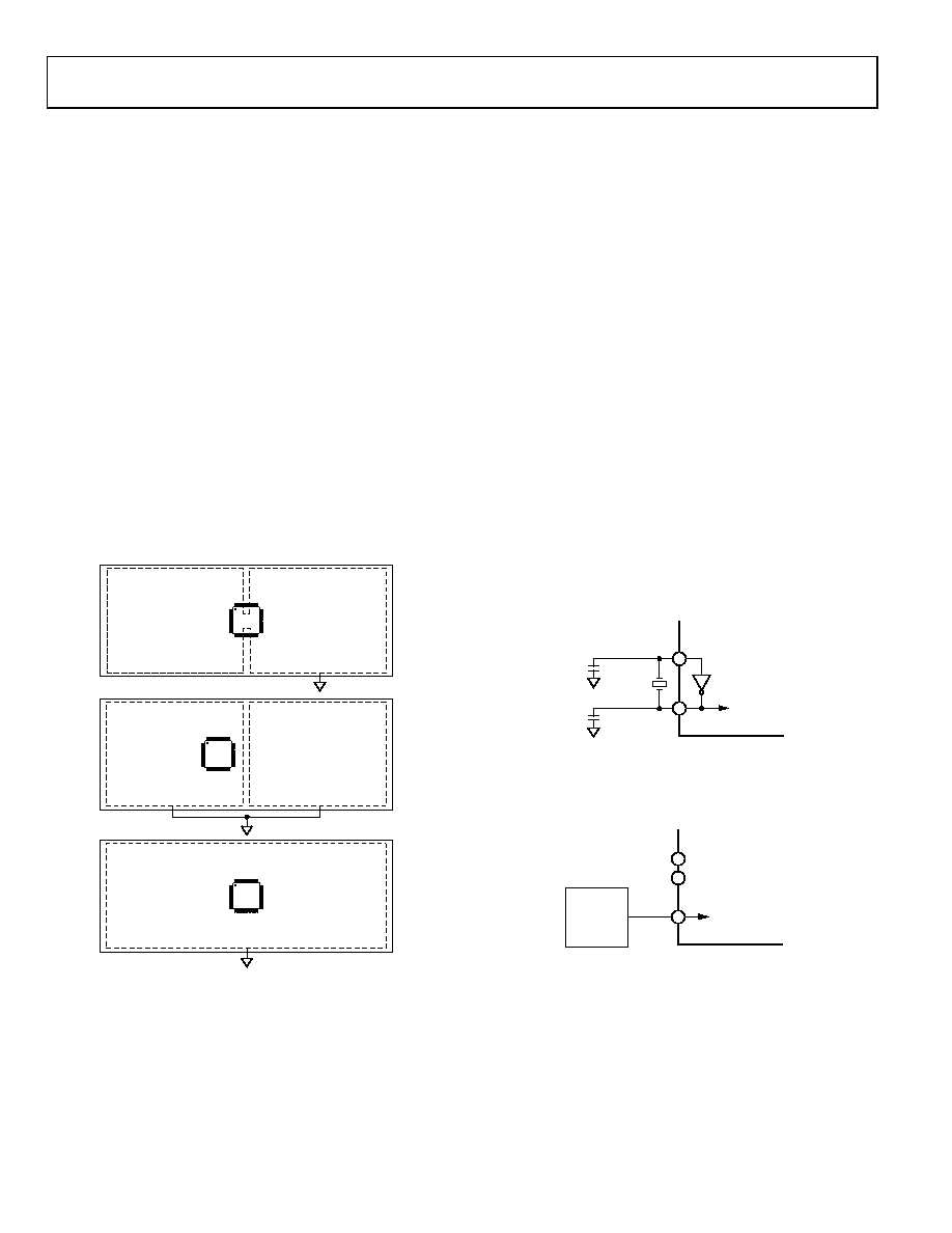
GROUNDING AND BOARD LAYOUT
RECOMMENDATIONS
As with all high resolution data converters, special attention
must be paid to grounding and PC board layout of the
ADuC7124/ADuC7126-based designs to achieve optimum
performance from the ADCs and DAC.
Although the part has separate pins for analog and digital ground
(AGND and IOGND), the user must not tie these to two sepa-
rate ground planes unless the two ground planes are connected
very close to the part. This is illustrated in the simplified example
shown in Figure 66a. In systems where digital and analog
ground planes are connected together somewhere else (at the
power supply of the system, for example), the planes cannot be
reconnected near the part because a ground loop results. In these
cases, tie all the ADuC7124/ADuC7126 AGND and IOGND
pins to the analog ground plane, as illustrated in Figure 66b.
In systems with only one ground plane, ensure that the digital
and analog components are physically separated onto separate
halves of the board so that digital return currents do not flow
near analog circuitry (and vice versa).
The ADuC7124/ADuC7126 can then be placed between the
digital and analog sections, as illustrated in Figure 66c.
09
12
3-
0
47
a.
PLACE ANALOG
COMPONENTS HERE
PLACE DIGITAL
COMPONENTS HERE
AGND
DGND
b.
PLACE ANALOG
COMPONENTS
HERE
PLACE DIGITAL
COMPONENTS HERE
AGND
DGND
c.
PLACE ANALOG
COMPONENTS HERE
PLACE DIGITAL
COMPONENTS HERE
DGND
Figure 66. System Grounding Schemes
In all of these scenarios, and in more complicated real-life
applications, the users should pay particular attention to the
flow of current from the supplies and back to ground. Make
sure the return paths for all currents are as close as possible to
the paths the currents took to reach their destinations.
For example, do not power components on the analog side (as
currents from IOVDD to flow through AGND. Avoid digital
currents flowing under analog circuitry, which can occur if a
noisy digital chip is placed on the left half of the board (shown
in Figure 66c). If possible, avoid large discontinuities in the
ground plane(s), such as those formed by a long trace on the same
layer, because they force return signals to travel a longer path.
In addition, make all connections to the ground plane directly,
with little or no trace separating the pin from its via to ground.
When connecting fast logic signals (rise/fall time < 5 ns) to any of
the ADuC7124/ADuC7126 digital inputs, add a series resistor to
each relevant line to keep rise and fall times longer than 5 ns at
the input pins of the part. A value of 100 Ω or 200 Ω is usually
sufficient to prevent high speed signals from coupling capaci-
tively into the part and affecting the accuracy of ADC conversions.
CLOCK OSCILLATOR
The clock source for the ADuC7124/ADuC7126 can be generated
by the internal PLL or by an external clock input. To use the
internal PLL, connect a 32.768 kHz parallel resonant crystal
between XCLKI and XCLKO, and connect a capacitor from
each pin to ground as shown in Figure 67. The crystal allows the
PLL to lock correctly to give a frequency of 41.78 MHz. If no
external crystal is present, the internal oscillator is used to give
a typical frequency of 32.768 kHz ± 3%.
09123
-048
ADuC7124/
ADuC7126
TO
INTERNAL
PLL
12pF
XCLKI
32.768kHz
12pF
XCLKO
Figure 67. External Parallel Resonant Crystal Connections
To use an external source clock input instead of the PLL (see
Figure 68), Bit 1 and Bit 0 of PLLCON must be modified. The
external clock uses P0.7 and XCLK.
09123
-049
ADuC7124/
ADuC7126
TO
FREQUENCY
DIVIDER
XCLKO
XCLKI
XCLK
EXTERNAL
CLOCK
SOURCE
Figure 68. Connecting an External Clock Source
Using an external clock source, the ADuC7124/ADuC7126
specified operational clock speed range is 50 kHz to 41.78 MHz
± 1%, which ensures correct operation of the analog peripherals
and Flash/EE.
相关PDF资料 |
PDF描述 |
|---|---|
| AT91SAM7SE32B-CUR | IC MCU ARM7 32KB FLASH 144LFBGA |
| VI-J3V-IW-F4 | CONVERTER MOD DC/DC 5.8V 100W |
| VI-J3V-IW-F3 | CONVERTER MOD DC/DC 5.8V 100W |
| VI-J3V-IW-F2 | CONVERTER MOD DC/DC 5.8V 100W |
| ADUC7024BCPZ62I-RL | IC MCU 12BIT 1MSPS ANLG 64LFCSP |
相关代理商/技术参数 |
参数描述 |
|---|---|
| ADUC7126BSTZ126 | 功能描述:IC MCU 16/32B 126KB FLASH 80LQFP RoHS:是 类别:集成电路 (IC) >> 嵌入式 - 微控制器, 系列:MicroConverter® ADuC7xxx 标准包装:250 系列:LPC11Uxx 核心处理器:ARM? Cortex?-M0 芯体尺寸:32-位 速度:50MHz 连通性:I²C,Microwire,SPI,SSI,SSP,UART/USART,USB 外围设备:欠压检测/复位,POR,WDT 输入/输出数:40 程序存储器容量:96KB(96K x 8) 程序存储器类型:闪存 EEPROM 大小:4K x 8 RAM 容量:10K x 8 电压 - 电源 (Vcc/Vdd):1.8 V ~ 3.6 V 数据转换器:A/D 8x10b 振荡器型:内部 工作温度:-40°C ~ 85°C 封装/外壳:48-LQFP 包装:托盘 其它名称:568-9587 |
| ADUC7126BSTZ126I | 功能描述:IC MCU 16/32B 126KB FLASH 80LQFP RoHS:是 类别:集成电路 (IC) >> 嵌入式 - 微控制器, 系列:MicroConverter® ADuC7xxx 标准包装:250 系列:LPC11Uxx 核心处理器:ARM? Cortex?-M0 芯体尺寸:32-位 速度:50MHz 连通性:I²C,Microwire,SPI,SSI,SSP,UART/USART,USB 外围设备:欠压检测/复位,POR,WDT 输入/输出数:40 程序存储器容量:96KB(96K x 8) 程序存储器类型:闪存 EEPROM 大小:4K x 8 RAM 容量:10K x 8 电压 - 电源 (Vcc/Vdd):1.8 V ~ 3.6 V 数据转换器:A/D 8x10b 振荡器型:内部 工作温度:-40°C ~ 85°C 封装/外壳:48-LQFP 包装:托盘 其它名称:568-9587 |
| ADUC7126BSTZ126IRL | 功能描述:IC MCU 16/32B 126KB FLASH 80LQFP RoHS:是 类别:集成电路 (IC) >> 嵌入式 - 微控制器, 系列:MicroConverter® ADuC7xxx 标准包装:38 系列:Encore!® XP® 核心处理器:eZ8 芯体尺寸:8-位 速度:5MHz 连通性:IrDA,UART/USART 外围设备:欠压检测/复位,LED,POR,PWM,WDT 输入/输出数:16 程序存储器容量:4KB(4K x 8) 程序存储器类型:闪存 EEPROM 大小:- RAM 容量:1K x 8 电压 - 电源 (Vcc/Vdd):2.7 V ~ 3.6 V 数据转换器:- 振荡器型:内部 工作温度:-40°C ~ 105°C 封装/外壳:20-SOIC(0.295",7.50mm 宽) 包装:管件 其它名称:269-4116Z8F0413SH005EG-ND |
| ADUC7126BSTZ126-RL | 功能描述:IC MCU 16/32B 126KB FLASH 80LQFP RoHS:是 类别:集成电路 (IC) >> 嵌入式 - 微控制器, 系列:MicroConverter® ADuC7xxx 标准包装:38 系列:Encore!® XP® 核心处理器:eZ8 芯体尺寸:8-位 速度:5MHz 连通性:IrDA,UART/USART 外围设备:欠压检测/复位,LED,POR,PWM,WDT 输入/输出数:16 程序存储器容量:4KB(4K x 8) 程序存储器类型:闪存 EEPROM 大小:- RAM 容量:1K x 8 电压 - 电源 (Vcc/Vdd):2.7 V ~ 3.6 V 数据转换器:- 振荡器型:内部 工作温度:-40°C ~ 105°C 封装/外壳:20-SOIC(0.295",7.50mm 宽) 包装:管件 其它名称:269-4116Z8F0413SH005EG-ND |
| ADUC7128 | 制造商:AD 制造商全称:Analog Devices 功能描述:Precision Analog Microcontroller ARM7TDMI MCU with 12-bit ADC & DDS DAC |
发布紧急采购,3分钟左右您将得到回复。